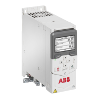
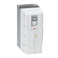
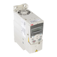
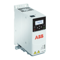
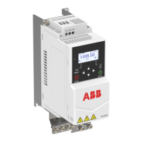
The ACSM1-04
20
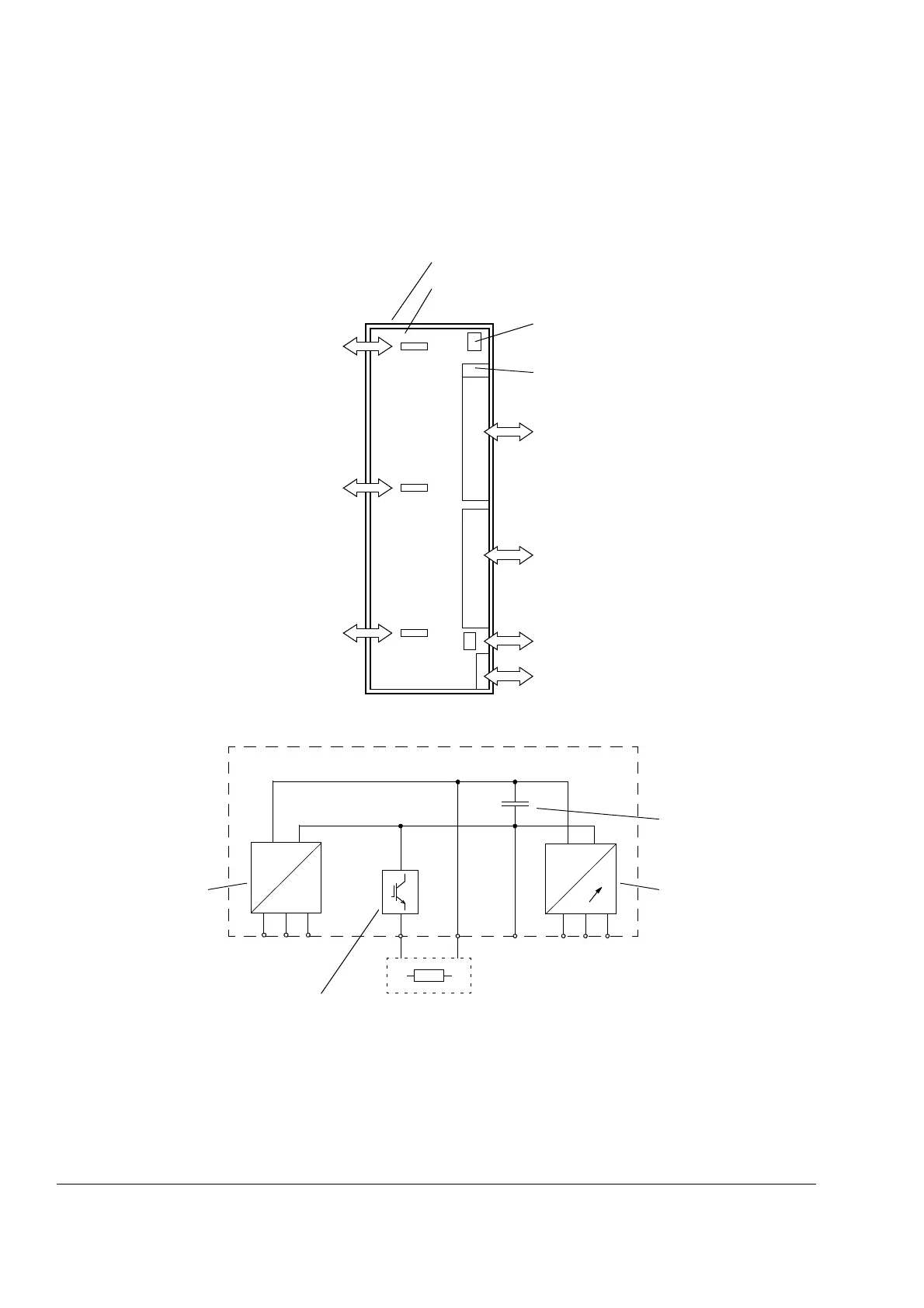
Main circuit and control interfaces
The diagram below shows the control interfaces and the main circuit of the drive. For
further information on the JCU Control Unit, see the chapter Electrical installation.
Option 1
Digital or analogue I/O extension
(FIO-01, FIO-11)
Incremental or absolute encoder interface, or
resolver interface (FEN-01, FEN-11, FEN-21)
Option 3
Fieldbus adapter (FPBA-0x, FCAN-0x,
FDNA-0x, FENA-0x etc.)
Slot 1
Power unit
Slot 2
Slot 3
Control unit (JCU), installed onto the power unit
Digital I/O
Analogue I/O
Thermistor input
Drive-to-drive link
Safe Torque Off connection
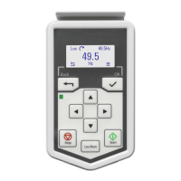
Control panel (optional) or PC connection
Memory unit (JMU) containing the
application program (see page 69)
7-segment status display (see page 69)
Option 2
Connectivity as with Option 1 above.
Note: No two I/O extensions or feedback
interfaces of the same type can be
connected at a time.
External 24 V power input (see page 60)
Motor output
Braking chopper
+–
~
=
ACSM1-04
Rectifier
Capacitor bank
Braking resistor
(optional)
~
=
AC supply
V1 W1U1
R-
UDC+
R+
UDC-
V2 W2U2
Inverter
 Loading...