— 19 —
LSI MON
SWO
LSO
" L "
" H "
GNDVDD
CSB
" H "
FROM CPU
CS2 terminal
(Pin 28)
(Pin 25)(Pin 26)
(Pin 40)
(Pin 24)
TO CPU
TO MAIN SWITCH
"L"
"H"
OFF
ON
SWO
SW
CPU
GATE ARRAY
MAIN SWITCH
VDD
"L"
"L"
KAC
KIO
(Pin36)
(Pin40)
(Pin54)
(Pin53)
POWER ON SWITCH
(Pin 27)
(Pin 70)
INT0 terminal
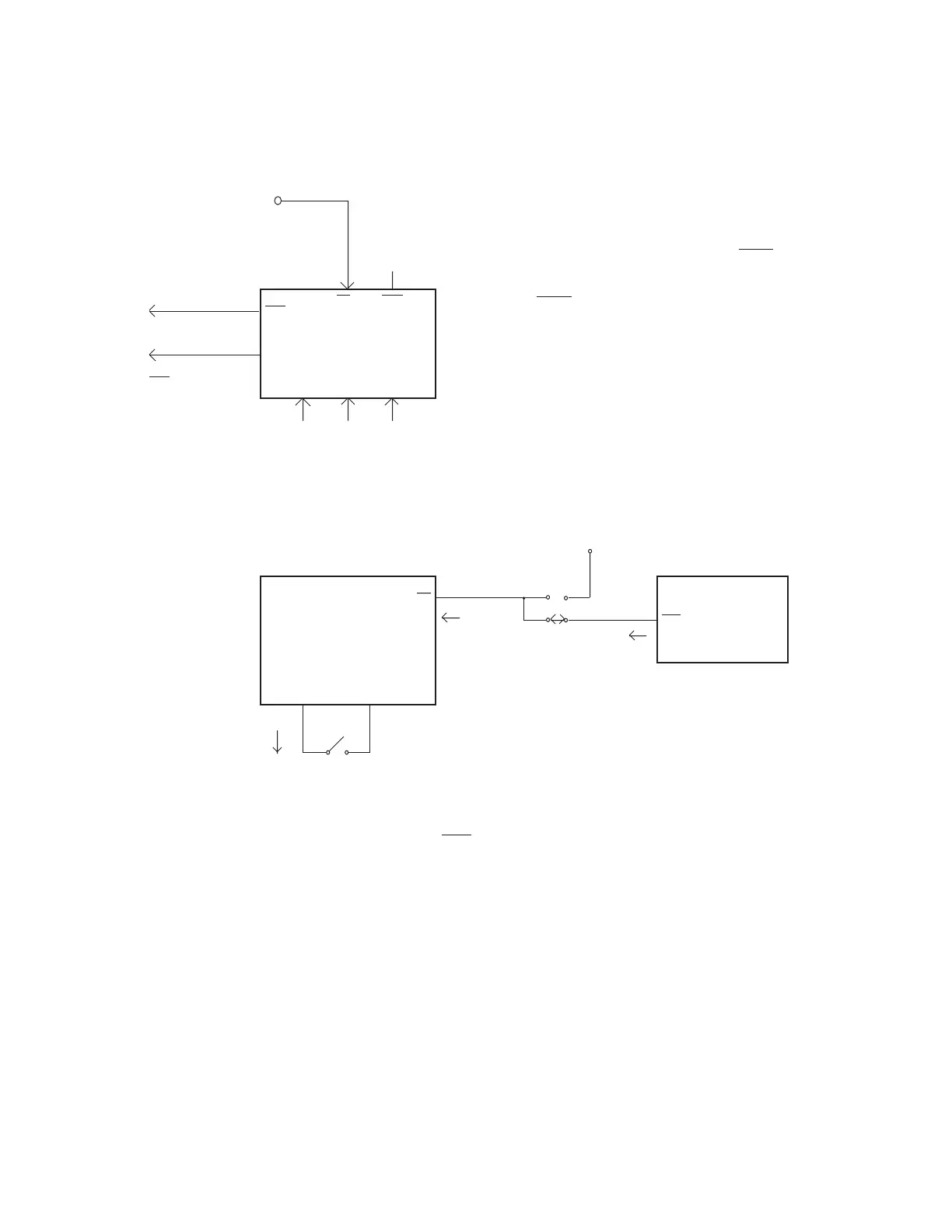
8) Gate array
9) Main switch and power on switch
When the main switch is set to on position, SW terminal of CPU becomes "L", then CPU will send "L"
signal to KAC terminal to enable the system power on. The KI0 terminal is "H" when VDD is applied to
CPU. Therefore, when pressing the power on switch, CPU will generate a clock pulse (2 MHz) for start
up the system.
µPD65005GC-566-3B6
HD62076C02
GATE ARRAY
µPD65005GC-566-3B6
GND
Open
(Pin 34)
(Pin 33)
(Pin 7)
When VDD is applied from power supply IC
SC371015FU to gate array µPD65005GC-556-
3B6, gate array will send "L" signal to active the
main switch signal from terminal SWO.
Also, gate array will send "H" signal to release
the INT0 terminal of CPU from LSO terminal.
The terminal CSB is for the chip select of gate
array. This signal is sent from CPU terminal
CS2. And when the VDD is applied to CPU, CPU
will send "H" signal to CSB terminal.
 Loading...