— 20 —
VDD
VOB
DATA
ADDRESS
HD62076C02
CPU
VCC
" L "
VDD
R10
(Pin3)
(Pin1)
(Pin2)
VOT
VIN
"H"
V2ON
INT1
CPU
PDB
SC371015FU
(Pin45) (Pin31)
(Pin32) (Pin31)
LCD drive voltages
VREG,V1~V4
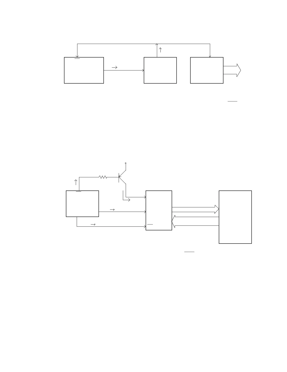
When the system is start up, CPU will send "H" signal to VIN terminal of gate array from V2ON termi-
nal. Then, gate array will send "H" signal from VOT terminal to release interruption signal INT1 of CPU
and also, it will be sent to PDB terminal of power supply chip to generate LCD drive voltages.
After gate array send VOT signal, gate array send "L" signal from VOB terminal to base terminal of
transistor Q1. Then, the VDD is applied to ROM (operation program), CPU can read a ROM program
data.
10) Power supply for LCD
11) ROM driving transistor
HD62076C02
GATE ARRAY
OEB
(Pin43) (Pin24)
"H"
Transistor Q1
2SA1411
(Pin39)
(Pin32)
(Pin69)
µPD65005GC-566-3B6
GATE ARRAY
POWER SUPPLY CHIP
OEO
RSO
ROM
µPD23C4001
EBGW-304
CEB
"Pulse"
µPD65005GC-566-3B6
"Pulse"
(Pin49)
(Pin22)
 Loading...