26
7. Check 5V
(5.2V VBUS power for DOCK)
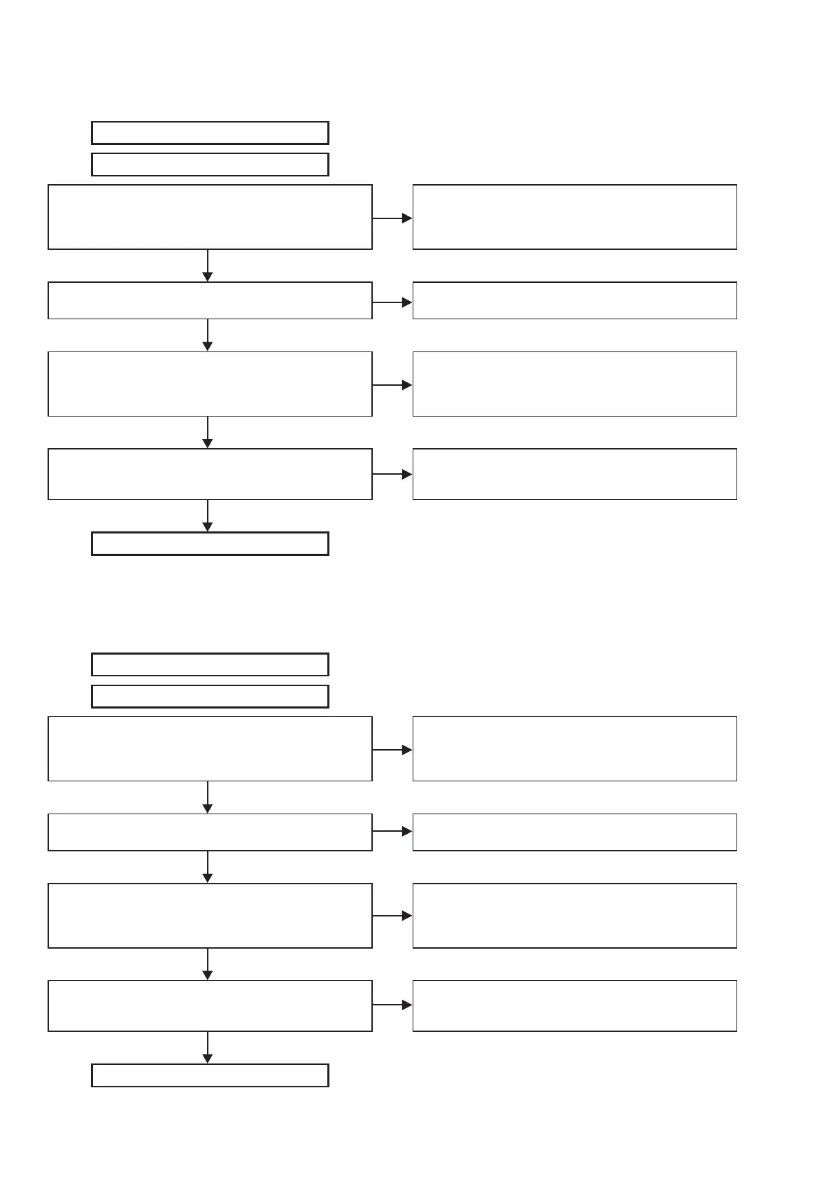
Start (MAIN PWB)
Preparing: Release (Q11)
U8(2pin) input voltage check, spec 12V±10%
Is the voltage in the spec?
U8 output enable (7pin) H?
U8 PWM output wave check (3pin)
5V output voltage check (C66), spec 5.15V-5.25V
Is the voltage in the spec?
1. Soldering check of (U8, R55, C67, C77)
2. After release (R55), conduct check of (C67, C77)
3. Return to check "12V"
Return to check "VMCU"
1. Soldering check of (U8, C74, L10, R74, R70, C66, C78)
2. After release(R63), conduct check of (C66, C78)
3. Replace (C74→MAIN PWB assy)
1. Soldering check of (U8, L10, C74, R74, R70)
2. Replace (C74→MAIN PWB assy)
NO
NO
NO
NO
YES
YES
YES
YES
Finish
8. Check ADSP_1V1
(1.1V DSP power)
U7(4pin) input voltage check, spec 12V±10%
Is the voltage in the spec?
U7 output enable (1pin) H?
U7 PWM output wave check (3pin)
1.1V output voltage check (R72), spec 1.1V±5%
Is the voltage in the spec?
1. Soldering check of (U7, R71, C69, C70)
2. After release (R71), conduct check of (C69, C70)
3. Return to check "12V"
Return to check "VMCU"
1. Soldering check of (U7, L9, R76, R82, C71, C72, C73)
2. After release(R72), conduct check of (C71, C72, C73)
3. Replace MAIN PWB assy
1. Soldering check of (U7, L9, R76, R82)
2. Replace MAIN PWB assy
NO
NO
NO
NO
YES
YES
YES
YES
Preparing: Release (Q20)
Start (MAIN PWB)
Finish