51
SEMICONDUCTORS
Only major semiconductors are shown. General semiconductors etc. are omitted from list.
The semiconductors which have a detailed drawing in a schematic diagram are omitted from list.
IC's
MSP430G2202IPW20R_(U1)
MSP430G2202IPW20R_(U1) Terminal Functions
1
DVCC
2
P1.0/TA0CLK/ACLK/A0
3
4
5
P1.3/ADC10CLK/VREF-/VEREF-/A3
6
7
8
P2.0
9
P2.1
10
P2.2
11
P2.3
12
P2.4
13
P2.5
14
15
16
RST/NMI/SBWTDIO
17
TEST/SBWTCK
18
XOUT/P2.7
19
XIN/P2.6/TA0.1
20
DVSS
P1.6/TA0.1/ TDI/TCLKSDO/SCL/A6/
P1.7/SDI/SDA/A7/TDO/TDI
P1.1/TA0.0/A1
P1.2/TA0.1/A2
P1.4/TA0.2/SMCLK/A4/ /TCK
VREF+/VEREF+
P1.5/TA0.0 A5/TMS/SCLK/
1
2
3
4
5 6 7 8
9
RST/NMI/SBWTDIO
10 TEST/SBWTCK
11 XOUT/P2.7
12 XIN/P2.6/TA0.1
13
AVSS
14
DVSS
15
AVCC
16
DVCC
P1.0/TA0CLK/ACLK/A0
P1.3/ADC10CLK/A3/VREF-/VEREF-
P1.6/TA0.1/SDO/SCL/A6TDI/TCLK/
P1.7/ /TDO/TDISDI/SDA/A7
P1.1/TA0.0/A1
P1.2/TA0.1/A2
P1.4/SMCLK/A4/VREF+/VEREF+/TCK
P1.5/TA0.0/SCLK/A5/TMS
1
DVCC
2
3
4
5
6
7
8
9
10
RST/NMI/SBWTDIO
11
TEST/SBWTCK
12
XOUT/P2.7
13
XIN/P2.6/TA0.1
14
DVSS
P1.0/TA0CLK/ACLK/A0
P1.3/ADC10CLK/A3/VREF-/VEREF-
P1.6/TA0.1/SDO/SCL/A6/TDI/TCLK
P1.7 /TDO/TDI/SDI/SDA/A7
P1.1/TA0.0/A1
P1.2/TA0.1/A2
P1.4/TA0.2/SMCLK/A4/VREF+/VEREF+/TCK
P1.5/TA0.0/SCLK/A5/TMS
MSP430G2x32
MSP430G2x02
www.ti.com
SLAS723F –DECEMBER 2010 –REVISED MAY 2012
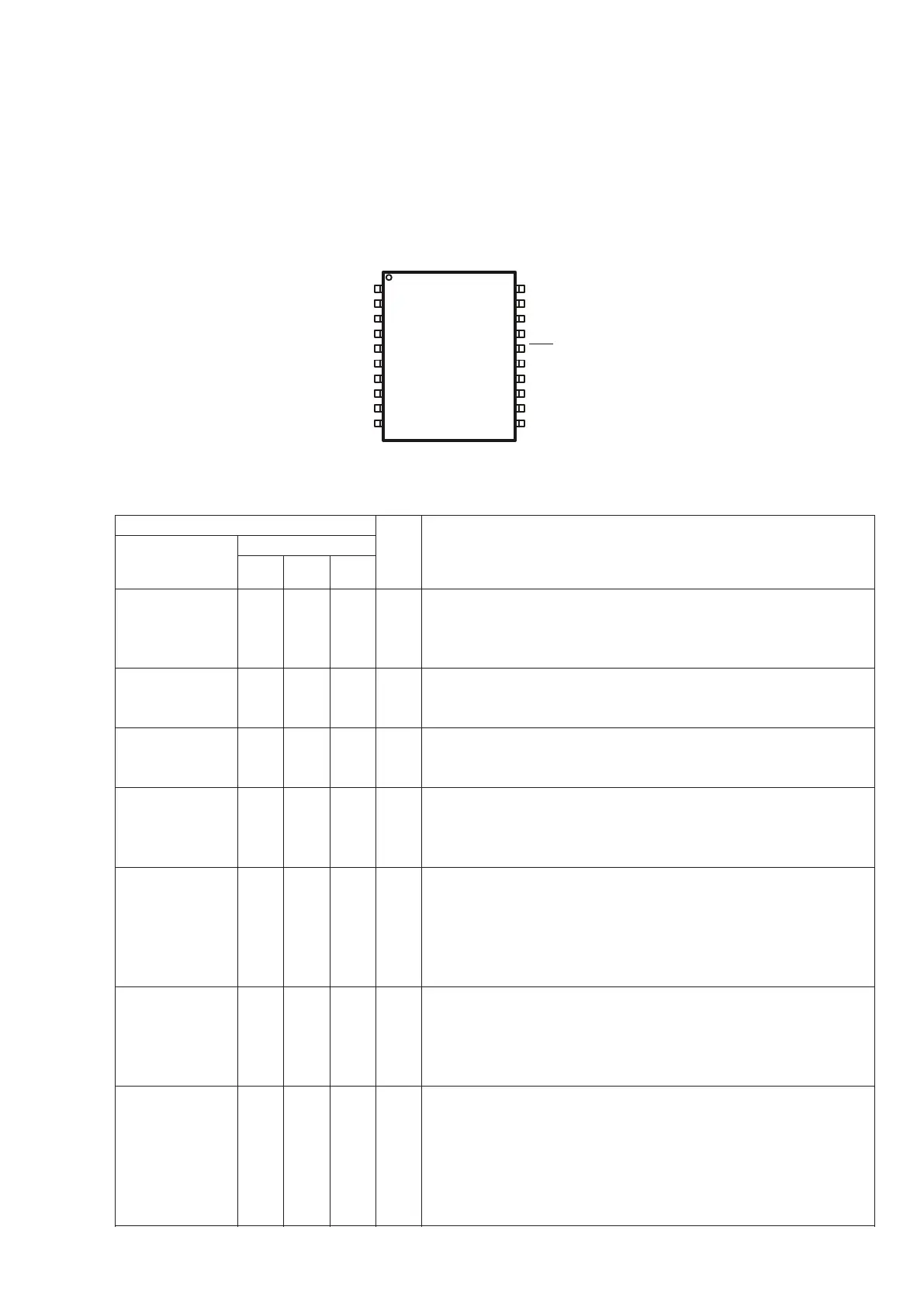
DEVICE PINOUTS
PW PACKAGE
(TOP VIEW)
NOTE: ADC10 pin functions are available only on MSP430G2x32.
NOTE: The pulldown resistors of port pins P2.0, P2.1, P2.2, P2.3, P2.4, and P2.5 should be enabled by setting P2REN.x = 1.
RSA PACKAGE
(TOP VIEW)
NOTE: ADC10 pin functions are available only on MSP430G2x32.
NOTE: The pulldown resistors of port pins P2.0, P2.1, P2.2, P2.3, P2.4, and P2.5 should be enabled by setting P2REN.x = 1.
N OR PW PACKAGE
(TOP VIEW)
NOTE: ADC10 pin functions are available only on MSP430G2x32.
Copyright © 2010–2012, Texas Instruments Incorporated
Submit Documentation Feedback 3
MSP430G2x32
MSP430G2x02
www.ti.com
SLAS723F –DECEMBER 2010 –REVISED MAY 2012
TERMINAL FUNCTIONS
Table 2. Terminal Functions
TERMINAL
NO.
I/O DESCRIPTION
NAME
N14, RSA1 N20,
PW14 6 PW20
P1.0/ General-purpose digital I/O pin
TA0CLK/ Timer0_A, clock signal TACLK input
2 1 2 I/O
ACLK/ ACLK signal output
A0 ADC10 analog input A0
(1)
P1.1/ General-purpose digital I/O pin
TA0.0/ 3 2 3 I/O Timer0_A, capture: CCI0A input, compare: Out0 output
A1 ADC10 analog input A1
(1)
P1.2/ General-purpose digital I/O pin
TA0.1/ 4 3 4 I/O Timer0_A, capture: CCI1A input, compare: Out1 output
A2 ADC10 analog input A2
(1)
P1.3/ General-purpose digital I/O pin
ADC10CLK/ ADC10, conversion clock output
(1)
5 4 5 I/O
A3/ ADC10 analog input A3
(1)
VREF-/VEREF ADC10 negative reference voltage
(1)
P1.4/ General-purpose digital I/O pin
TA0.2/ Timer0_A, capture: CCI2A input, compare: Out2 output
SMCLK/ SMCLK signal output
6 5 6 I/O
A4/ ADC10 analog input A4
(1)
VREF+/VEREF+/ ADC10 positive reference voltage
(1)
TCK JTAG test clock, input terminal for device programming and test
P1.5/ General-purpose digital I/O pin
TA0.0/ Timer0_A, compare: Out0 output
A5/ 7 6 7 I/O ADC10 analog input A5
(1)
SCLK/ USI: clk input in I2C mode; clk in/output in SPI mode
TMS JTAG test mode select, input terminal for device programming and test
P1.6/ General-purpose digital I/O pin
TA0.1/ Timer0_A, compare: Out1 output
A6/ ADC10 analog input A6
(1)
SDO/ 8 7 14 I/O USI: Data output in SPI mode
SCL/ USI: I2C clock in I2C mode
TDI/ JTAG test data input or test clock input during programming and test
TCLK
P1.7/ General-purpose digital I/O pin
A7/ ADC10 analog input A7
(1)
SDI/ 9 8 15 I/O USI: Data input in SPI mode
SDA/ USI: I2C data in I2C mode
TDO/TDI
(2)
JTAG test data output terminal or test data input during programming and test
P2.0 - - 8 I/O General-purpose digital I/O pin
P2.1 - - 9 I/O General-purpose digital I/O pin
P2.2 - - 10 I/O General-purpose digital I/O pin
P2.3 - - 11 I/O General-purpose digital I/O pin
(1) Available only on MSP430G2x32 devices.
(2) TDO or TDI is selected via JTAG instruction.
Copyright © 2010–2012, Texas Instruments Incorporated
Submit Documentation Feedback 5