APEX™ Exciter Incorporating FLO™ Technology
Exciter Troubleshooting Maintenance and Troubleshooting
2604s500.fm
03/08/07 888-2604-001 Page: 5-25
WARNING: Disconnect primary power prior to servicing.
5.8.7 Analog Tray Troubleshooting
A brief outline of troubleshooting topics is included below. The RF input and output levels
for the analog tray are listed in Table 5-4.
• Exciter loopback test.
Loopback tests are covered in Section 5.8.5, Isolating Problem to the Analog or Digi-
tal Tray, on page 5-21.
• Frequency test.
Frequency topics are covered in Section 5.1.2, Measuring PLL Board Frequencies, on
page 5-6, Section 5.1.2.1, Measuring Center Channel Frequency, on page 5-6, and in
Section 5.8.1, Frequency Error, on page 5-19.
• Check dc supply voltages to each board.
Power supply topics are covered in Section 5.8.3, Power Supply Voltages, on
page 5-20 and in Section 4.5.3, Analog Deck Power, on page 4-16.
• Output power level (check power calibration). Power calibration is covered in Section
3.6.2.1 on page 3-38.
• Measure signal levels and signal frequencies at the inputs and outputs of each board.
See Table 5-4 for a list of input and output signal levels.
Analog board frequency measurements are covered in Section 5.1.2 on page 5-6.
• Measure the PM noise of the CW signal outputs of the PLL board, see Table 5-5,
Phase Noise Mask.
• Observe the spectral response at the signal inputs and outputs of the up converter and
the output amplifier with both RTAC samples set to bypass.
Figure 5-9 shows the spectral response at the output of the exciter with both RTAC
functions bypassed. Table 5-6 lists the actual bandwidth for each bandwidth setting.
The modulator bandwidth is set in the Setup > Flo FPGA > FPGA Configure 4/5
screen.
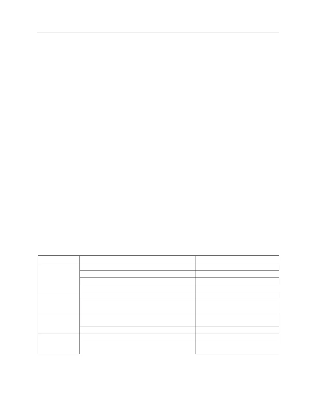
Table 5-4 Analog Tray RF Input and Output levels
Board Function and Connector Level
PLL First local oscillator output, J9 and J10 +10 dBm +3/-1 dB
Second local oscillator output, J5 and J6 +10 dBm +3/-1 dB
10 kHz reference input, J3 Not used
10 MHz reference output, J8 and J11 Not used
Up converter On channel RF output level, J14 -63 to -6 dBm
11.1 MHz first IF input, J4 +10 dBm peak +/-0.3 dB using two
tone test
Output Amplifier On channel RF output level, J2 26 to 30 dB gain, Up to 250 mW
average power
On channel RF output sample (to down converter), J4 -30 to 0 dBm
Down converter 11.1 MHz output (to ADC board), J5 -10 to -5 dBm
Exciter input J4, IPA input J3 (not used), PA input J2,
HPF input J1
Each input is -30 to 0 dBm
 Loading...