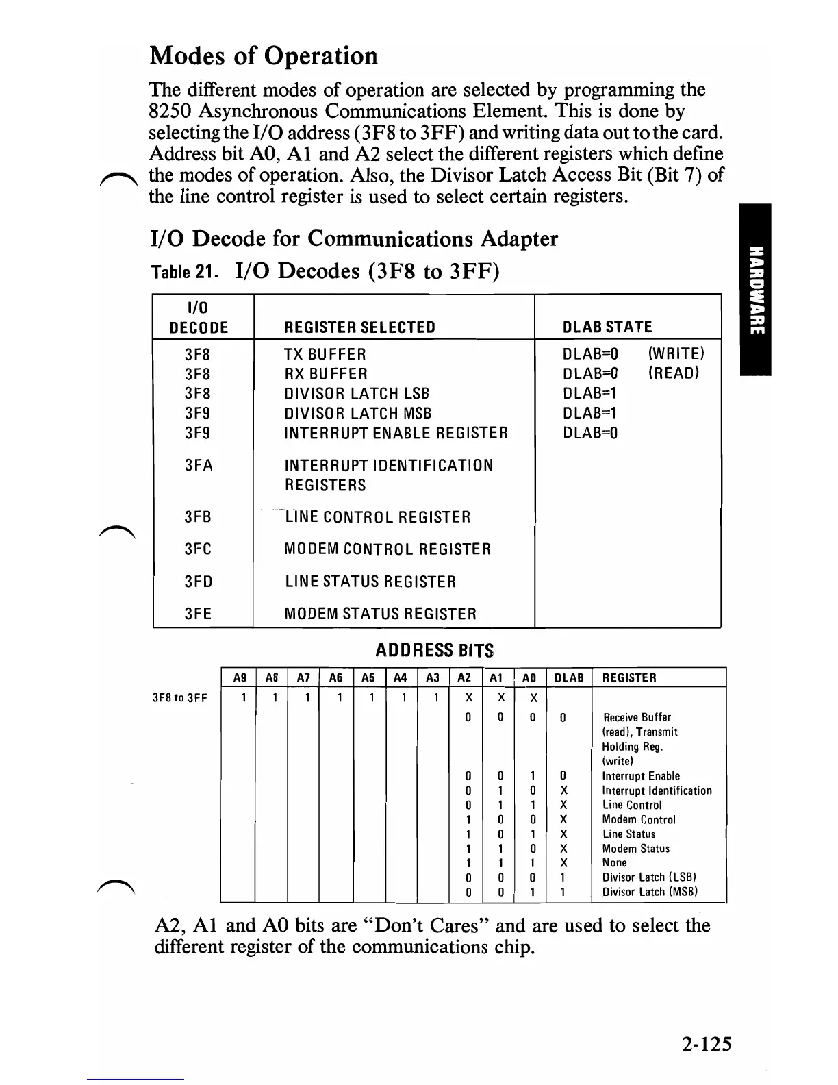
Modes
of
Operation
The different modes of operation are selected by programming the
8250 Asynchronous Communications Element. This
is
done by
selecting the
I/O address (3F8 to
3FF)
and writing data out to the card.
Address bit
AO,
Al
and A2 select the different registers which define
r"'\
the modes of operation. Also, the Divisor Latch Access Bit (Bit 7) of
the line control register
is
used to select certain registers.
I/O
Decode for Communications Adapter
Table
21.
I/O
Decodes (3F8 to
3FF)
I/O
DECODE
REGISTER
SELECTED
DLABSTATE
3FB
TX
BUFFER
DLAB=O
(WRITE)
3FB
RX
BUFFER
DLAB=O
(READ)
3FB
DIVISOR
LATCH
LSB
DLAB=l
3F9
DIVISOR
LATCH
MSB
DLAB=l
3F9
INTERRUPT
ENABLE
REGISTER
DLAB=O
3FA
INTERRUPT
IDENTIFICATION
REGISTERS
3FB
LINE
CONTROL
REGISTER
3FC
MODEM
CONTROL
REGISTER
3FD
LINE
STATUS
REGISTER
3FE
MODEM
STATUS
REGISTER
ADDRESS
BITS
A9 A8
A7
A6
A5
A4
A3 A2
A1
AD
DLAB
REGISTER
3F8
to
3FF
1 1 1
1
1
1 1
X X X
0 0 0
0
Receive
Buffer
(read), Transmit
Holding
Reg.
(write)
0
0
1
0
Interrupt
Enable
0
1 a x
Interrupt Identification
0
1 1
X
Li
ne
Control
1 a 0
X
Modem
Control
1 0
1
X
Line
Status
1
1
a
X
Modem
Status
1
1 1
X
None
0 a 0
1
Divisor
Latch
(LSB)
0 0
1 1
Divisor
Latch
(MSB)
A2,
Al
and
AO
bits are
"Don't
Cares" and are used to select the
different register of the communications chip.
2-125
 Loading...