Cassette User Interface
The cassette interface control
is
implemented in software. (See FIRM-
WARE
Section). An 825 3 timer output
is
used to control the data to the
cassette recorder. This output exits the System Board, at the rear,
through pin 5 of a
DIN
connector. The cassette input data
is
read by
an 8255A-5 Programmable Peripheral Interface (PPI) input port bit.
This signal
is
received through pin 4 of the cassette connector. Software
algorithms are used to generate and read cassette data. The casette
drive motor
is
controlled through pins 1 & 3
of
the cassette connector.
The motor on/off
is
controlled by an 8255A-PPI output port bit.
(Port '61 H', bit 3). The 8255 A address and bit assignments are defined
in
the
I/O
Address Map page. On the following pages are read, write,
and motor control block diagrams.
Cassette Jumpers
A 2x2 Berg Pin and Jumper are used on the cassette
Data
Out line.
The jumper will allow the
Data
Out line to be used as a microphone
input (75 mv.) when the jumper
is
placed across M and C pins. An
auxiliary input
is
available when the jumper
is
placed across the A and
C pins. The auxiliary input provides a .68 volt input to the recorder.
Refer to System Board Component Diagram page (2-13) for cassette
jumper location.
M A M A
JUMPER
DIAGRAM
Mike·
75
Mv.
Aux·O.68V
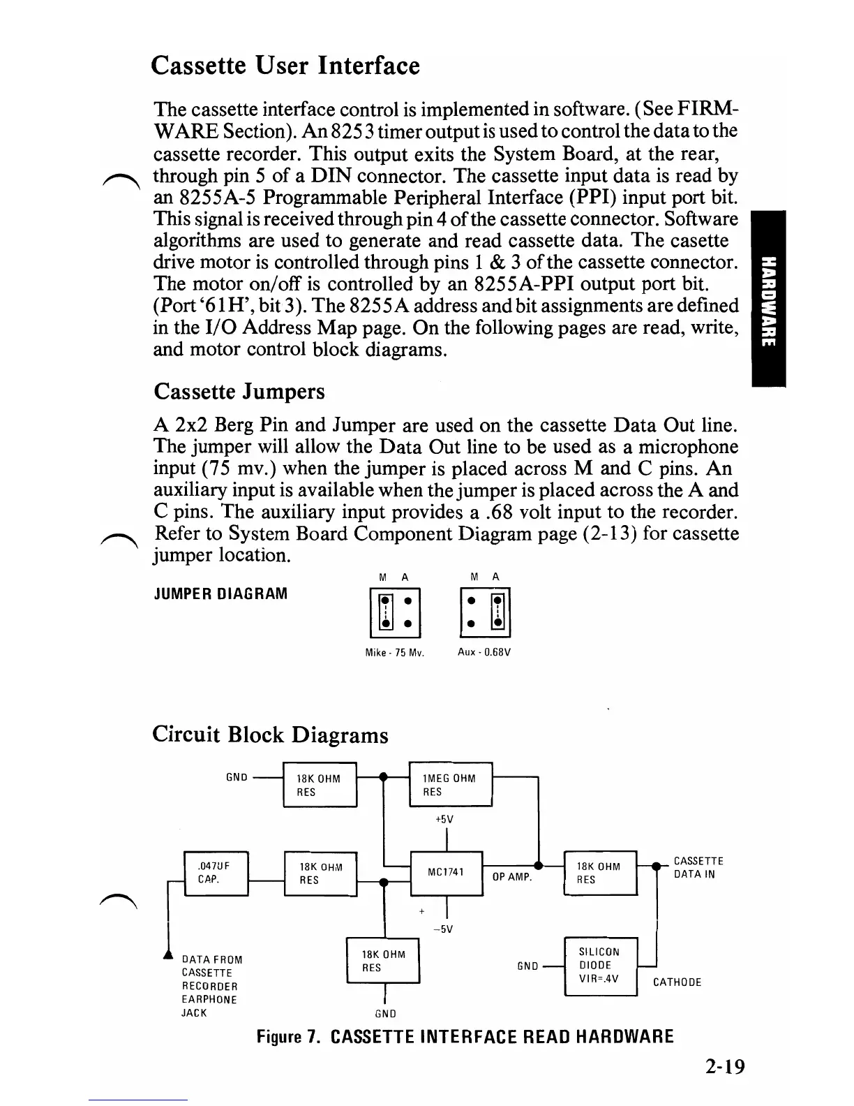
Circuit Block Diagrams
GND
+5V
CASSETTE
DATA
IN
SILICON
GND
DIODE
RECORDER
VIR=,4V
CATHODE
EARPHONE
JACK
GND
Figure
7.
CASSETTE
INTERFACE
READ
HARDWARE
2-19
 Loading...