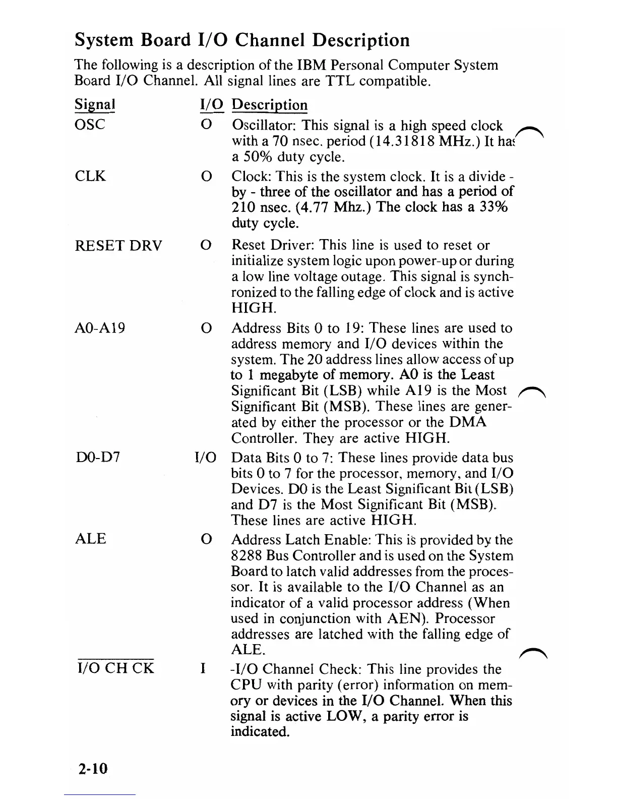
System Board I/O Channel Description
The following is a description
of
the
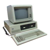
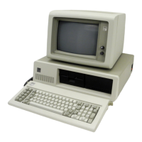
IBM
Personal Computer System
Board
I/O
Channel. All signal lines are
TTL
compatible.
Signal
I/O
Description
OSC
0 Oscillator: This signal is a high speed clock
r"\
with a 70 nsec. period (14.31818
MHz.)
It
hat
a
50% duty cycle.
CLK
0 Clock: This is the system clock.
It
is a divide -
by - three
of
the oscillator and has a period
of
210 nsec. (4.77 Mhz.)
The
clock has a
33%
duty cycle.
RESET
DRV
o Reset Driver: This line is used to reset or
initialize system logic upon power-up or during
a low line voltage outage. This signal is synch-
ronized to the falling edge
of
clock and
is
active
HIGH.
AO-AI9 o Address Bits 0
to
19: These lines are used to
address memory and
I/O
devices within the
system. The 20 address lines allow access
of
up
to
1 megabyte
of
memory.
AO
is
the Least
Significant Bit (LSB) while
A19
is the Most
r"\
Significant Bit (MSB). These lines are gener-
ated by either the processor or the
DMA
Controller. They are active
HIGH.
DO-D7
I/O
Data
Bits 0 to
7:
These lines provide
data
bus
bits
0 to 7 for the processor, memory, and
I/O
Devices.
DO
is the Least Significant Bit (LSB)
and
D7
is the Most Significant Bit (MSB).
These lines are active
HIGH.
ALE
o Address Latch Enable: This
is
provided by the
8288 Bus Controller and is used on the System
Board to latch valid addresses from the proces-
sor.
It
is available
to
the
I/O
Channel
as
an
indicator
of
a valid processor address (When
used in conjunction with
AEN).
Processor
addresses are latched with the falling edge
of
ALE.
r"\
I/O
CH
CK
I
-I/O
Channei Check: This line provides the
CPU
with parity (error) information on mem-
ory
or
devices in the
I/O
Channel.
When
this
signal is active
LOW,
a parity error is
indicated.
2-10
 Loading...