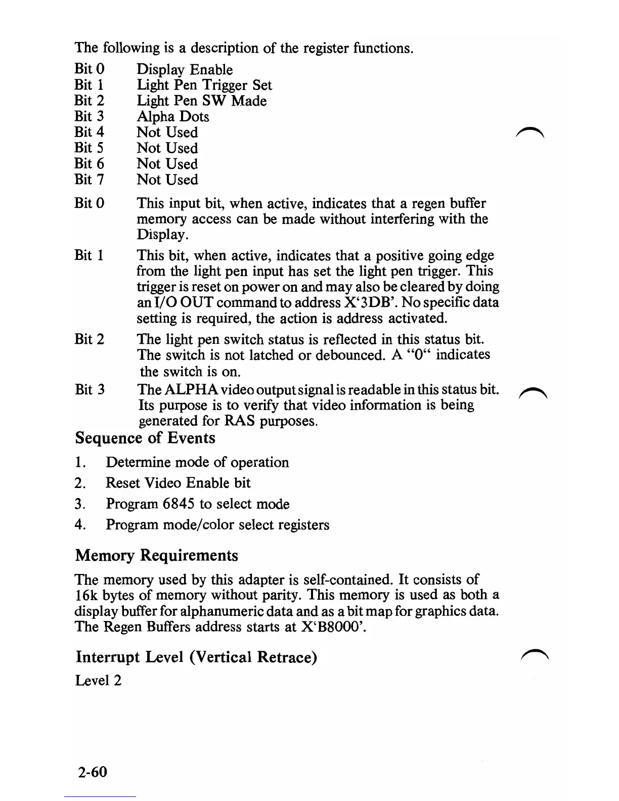
The following is a description
of
the register functions.
Bit 0 Display Enable
Bit 1 Light Pen Trigger Set
Bit 2 Light Pen
SW
Made
Bit 3 Alpha Dots
Bit 4
Not
Used
Bit 5
Not
Used
Bit
6
Not
Used
Bit
7
Not
Used
Bit 0 This input bit, when active, indicates that a regen buffer
memory access can be made without interfering with the
Display.
Bit
1 This bit, when active, indicates that a positive going edge
from the light pen input has set the light pen trigger. This
trigger is reset on power on and may also be cleared by doing
an
I/O
OUT
command to address
X'3DB'.
No
specific data
setting is required, the action is address activated.
Bit
2 The light pen switch status is reflected in this status bit.
The switch is not latched
or
debounced. A
"0"
indicates
the switch is on.
Bit 3 The
ALPHA
video output signal is readable in this status bit.
,.,.,.........
Its purpose
is
to verify that video information
is
being
generated for RAS purposes.
Sequence
of
Events
1.
Determine mode
of
operation
2. Reset Video Enable bit
3. Program 6845 to select mode
4. Program mode/color select registers
Memory Requirements
The memory used by this adapter is self-contained.
It
consists
of
16k bytes
of
memory without parity. This memory
is
used as both a
display buffer for alphanumeric data and as a bit map for graphics data.
The Regen Buffers address starts at X'B8000'.
Interrupt Level (Vertical Retrace)
Level 2
2-60
 Loading...