Chapter 2. Architecture and technical overview 35
Draft Document for Review May 28, 2009 1:59 pm 4405ch02 Architecture and technical overview.fm
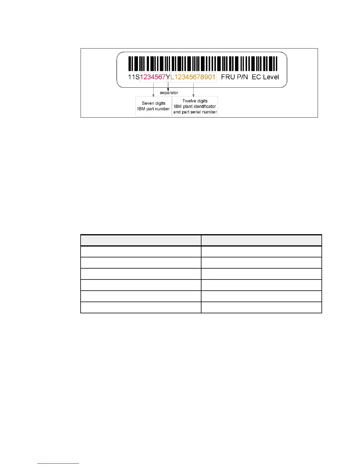
Figure 2-8 IBM memory certification label
2.4.5 Memory throughput
The memory subsystem throughput is based on the speed of the memory. On processor,
there are four memory channels, each with single 2 byte read and 1 byte write. Memory
channels of POWER6 memory controller are connected to Memory buffers. The processor
chip has two POWER6 processors. The DDR2 bus allows double reads or writes per clock
cycle. If a 667 MHz memory feature is selected, the throughput is (4 x 2 x 2 x 2 x 667) + (4 x 1
x 2 x 2 x 667) or 32016 MBps or 32 GBps. These values are maximum theoretical
throughputs for comparison purposes only.
Table 2-3 provides the theoretical throughput values of 4.7 GHz processors and 667 Mhz
memory configuration.
Table 2-3 Theoretical throughput values
2.5 System buses
The following sections provide additional information related to the internal buses.
2.5.1 I/O buses and GX+ card
Each POWER6 processor provides a GX+ bus which is used to connect to an I/O subsystem
or Fabric Interface card. The processor card populating the first processor slot is connected to
the GX+ multifunctional host bridge chip which provides the following major interfaces:
One GX+ passthru bus:
GX+ passthru elastic interface runs at one half the frequency of the primary. It allows other
GX+ bus hubs to be connected into the system.
Memory Bandwidth
L1 (Data) 75.2 GB/sec
L2 / Chip 300.8 GB/sec
L3 / Chip 37.6 GB/sec
Memory / Chip 32 GB/sec
Inter-Node Buses (16-cores) 75.2 GB/sec
Intra-Node Buses (16-cores) 100.26 GB/sec
 Loading...