EasyManua.ls Logo

National Instruments 6368 User Manual

National Instruments 6368
278 pages
To Next Page IconTo Next Page
To Previous Page IconTo Previous Page
Page #124 background imageLoading...
Page #124 background image
6-14 | ni.com
Chapter 6 Digital I/O
• Counter n Internal Output
• Frequency Output
• DI Change Detection output
Several other internal signals can be routed to DO Sample Clock through internal routes. Refer
to Device Routing in MAX in the NI-DAQmx Help or the LabVIEW Help for more information.
Using an External Source
Use one of the following external signals as the source of DO Sample Clock:
• PFI <0..15>
•RTSI <0..7>
• PXI_STAR
• PXIe_DSTAR<A,B>
• Analog Comparison Event (an analog trigger)
Routing DO Sample Clock to an Output Terminal
You can route DO Sample Clock (as an active low signal) out to any PFI <0..15>, RTSI <0..7>,
or PXIe_DSTARC terminal.
Other Timing Requirements
The DO timing engine on your device internally generates DO Sample Clock unless you select
some external source. DO Start Trigger starts the timing engine and either the software or
hardware can stop it once a finite generation completes. When using the DO timing engine, you
can also specify a configurable delay from DO Start Trigger to the first DO Sample Clock pulse.
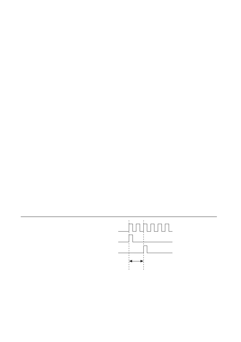
By default, this delay is two ticks of DO Sample Clock Timebase. Figure 6-7 shows the
relationship of DO Sample Clock to DO Start Trigger.
Figure 6-7. DO Sample Clock and DO Start Trigger
DO Sample Clock Timebase
DO Start Trigger
DO Sample Clock
Delay
From
Start
Trigger

Table of Contents

Questions and Answers:

National Instruments 6368 Specifications

General IconGeneral
Analog Input Channels16
Max Sample Rate2 MS/s
Resolution16-bit
Digital I/O Channels24
Counter/Timer Channels4
Analog Output Channels2
Analog Output Resolution16-bit
Digital I/O CompatibilityTTL
Input Range+/- 10 V
Bus TypePCIe
Operating System CompatibilityWindows, Linux

Summary

Chapter 1 Getting Started

Safety Guidelines

Precautions for safe operation and handling of NI 63xx devices, including EMC and symbol definitions.

Installation and Setup

Covers installing, unpacking, self-calibrating, mounting, and connecting X Series USB devices.

Device Pinouts and Specifications

Reference to appendix for pinouts and device specifications, plus accessory information.

Chapter 2 DAQ System Overview

DAQ Hardware and STC3

Details on DAQ hardware architecture and the DAQ-STC3 digital engine for X Series devices.

Calibration Circuitry

Information about the device's internal calibration circuitry for correcting gain and offset errors.

Cables and Accessories

Overview of available cables, connector blocks, and accessories for X Series devices.

Programming Devices in Software

Guidance on using NI-DAQmx driver software for programming DAQ devices.

Chapter 3 Connector and LED Information

I/O Connector Signal Descriptions

Detailed description of signals found on the I/O connectors of X Series devices.

+5 V Power Source and USER Terminals

Information on the +5V power source and USER 1/2 connections.

USB Device LED Patterns

Explanation of the behavior of the READY and ACTIVE LEDs on USB X Series devices.

Chapter 4 Analog Input

Analog Input Circuitry, Configuration, and Range

Covers analog input circuitry, terminal configurations, ranges, and voltage limits.

Data Acquisition Methods and Triggering

Explains acquisition methods and input triggering actions for analog signals.

Connecting Analog Input Signals

Guidance on connecting signals, including floating and ground-referenced sources.

Analog Input Timing Signals

Details on AI sample clock, convert clock, and other timing signals.

Chapter 5 Analog Output

Analog Output Circuitry and Reference Selection

Overview of AO circuitry, including DACs, FIFO, and reference selection for output range.

Output Signal Glitches and Generation Methods

Strategies for minimizing output glitches and details on generation methods.

Analog Output Triggering and Timing

Covers start/pause triggers and timing signals for analog output operations.

Chapter 6 Digital I/O

Digital I/O Features and Acquisition Methods

Overview of digital I/O, acquisition methods, and triggering for digital inputs.

Digital Waveform Acquisition and Generation

Details on acquiring and generating digital waveforms, including clock signals.

Digital Output Triggering and Generation Methods

Covers triggering and generation methods for digital outputs.

DI Change Detection and Digital Filtering

Information on detecting digital changes and applying programmable filters.

Chapter 7 Counters

Counter Timing Engine and Applications

Covers counter timing, input applications like edge counting, and pulse/frequency measurements.

Counter Output Applications and Timing Signals

Details counter output applications such as pulse generation and timing signal configurations.

Counter Triggering and Features

Information on counter triggering actions and features like cascading and prescaling.

Chapter 8 PFI

Using PFI Terminals for Timing Signals

Covers using PFI terminals for routing external timing input and output signals.

PFI for Static Digital I/O and Detection Events

Configuration of PFI terminals for static digital operations and detecting digital changes.

PFI Filters and I/O Protection

Details on applying filters to PFI signals and protecting I/O lines.

Chapter 9 Digital Routing and Clock Generation

Clock Routing and Timebases

Overview of clock routing circuitry, timebases, and external clock synchronization.

Synchronizing Multiple Devices

Methods for synchronizing devices across PXI Express, PCI Express, and USB platforms.

RTSI and PXI/PXI Express Signals

Details on RTSI signals, PXI/PXI Express clock/trigger signals, and PXI_STAR/PXIe_DSTAR.

Chapter 10 Bus Interface

Data Transfer Methods Overview

Introduction to data transfer methods across PCI Express, PXI Express, and USB.

PCI Express/PXI Express Data Transfer

Details DMA and Programmed I/O for PCI Express/PXI Express data transfer.

USB Data Transfer Methods

Details USB Signal Stream and Programmed I/O for USB data transfer.

Chapter 11 Triggering

Triggering with Digital and Analog Sources

Configuring triggers using digital signals and analog sources like AI channels or APFI.

Analog Trigger Actions and Types

Details actions affected by analog triggers and different trigger modes like edge, hysteresis, and window.

Improving Analog Trigger Accuracy

Tips for enhancing analog trigger accuracy using AI channels and software calibration.

Appendix A Device-Specific Information

NI 6320 Pinout and Specifications

Pinout diagram, specifications, and accessory information for the NI 6320 device.

NI 6345/6355 Pinouts and Specifications

Pinout diagrams and specifications for NI 6345/6355 devices.

NI USB-6349 Screw Terminal Pinout

Pinout details for the NI USB-6349 Screw Terminal device.

NI 6375 Pinout

Pinout details for the NI PXIe-6375 device.

Appendix B Where to Go from Here

Example Programs and Documentation

Where to find example programs, NI-DAQmx help, and X Series device specifications.

Software Support and Resources

Guides for LabVIEW, LabVIEW NXG, LabWindows/CVI, and Microsoft Visual Studio.

ANSI C Support

Resources for developing instrumentation applications using ANSI C with NI-DAQmx.

Appendix C Troubleshooting

Analog Input Troubleshooting

Solutions for common analog input issues such as crosstalk and improper grounding.

Analog Output and Counter Issues

Troubleshooting common analog output glitches and counter signal connection problems.

Appendix D NI Services

NI Services Overview

Information on global services, training, and technical support offered by NI.

Maintenance, Calibration, and System Integration

Details on hardware services, calibration, and partner integration support.

Training and Technical Support Resources

Information on NI training programs and technical support resources.

Related product manuals