© National Instruments | 9-1
9
Digital Routing and Clock
Generation
The digital routing circuitry has the following main functions:
• Manages the flow of data between the bus interface and the acquisition/generation
sub-systems (analog input, analog output, digital I/O, and the counters). The digital routing
circuitry uses FIFOs (if present) in each sub-system to ensure efficient data movement.
• Routes timing and control signals. The acquisition/generation sub-systems use these
signals to manage acquisitions and generations. These signals can come from the following
sources:
– Your X Series device
– Other devices in your system through RTSI
– User input through the PFI terminals
– User input through the PXI_STAR terminal
• Routes and generates the main clock signals for the X Series device.
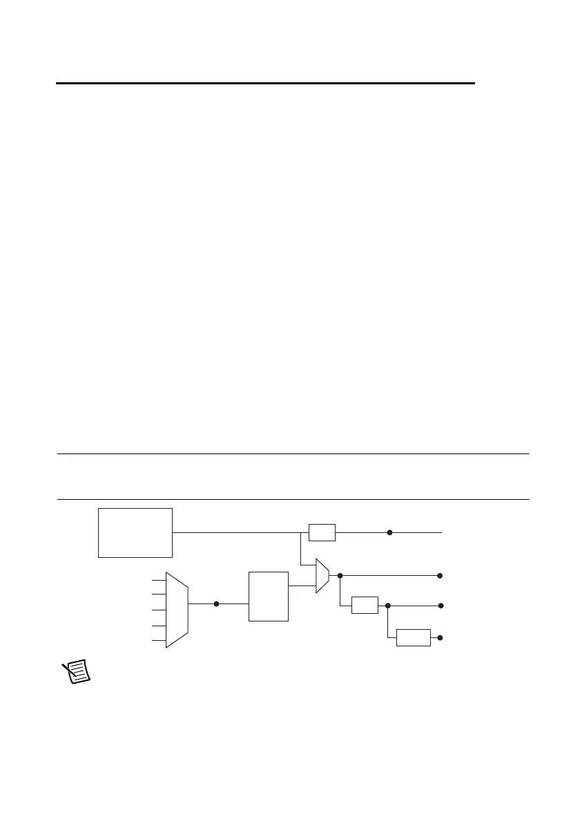
Clock Routing
Figure 9-1 shows the clock routing circuitry of an X Series device.
Figure 9-1. X Series Clock Routing Circuitry
Note (NI PXIe-6386/6396 Devices) PXIe-6386 and PXIe-6396 devices only
support PXIe_CLK100 and the onboard oscillator. For more information about
special considerations for these devices, go to ni.com/info and enter the Info
Code smio14ms.
RTSI <0..7>
Onboard
100 MHz
Oscillator
External
Reference
Clock
(To RTSI <0..7>
Output Selectors)
10 MHz RefClk
PLL
÷
5
÷
200
÷ 10
PXIe_CLK100
PXI_STA R
100 MHz
Timebase
100 kHz
Timebase
20 MHz
Timebase
PFI
PXIe-DSTAR<A, B>
 Loading...