EasyManuals Logo
Home>Nvidia>Control Unit>Jetson Orin Nano Series

Nvidia Jetson Orin Nano Series User Manual

Nvidia Jetson Orin Nano Series
99 pages
To Next Page IconTo Next Page
To Previous Page IconTo Previous Page
Page #45 background imageLoading...
Page #45 background image
USB and PCIe
PRELIMINARY INFORMATION
Jetson Orin NX Series and Jetson Orin Nano Series DG-10931-001_v1.1 | 34
Parameter
Requirement
Units
Notes
General: See Chapter 17 for guidelines related to serpentine routing, routing over voids and noise coupling
The following figures show the USB 3.2. Interface signal routing requirements.
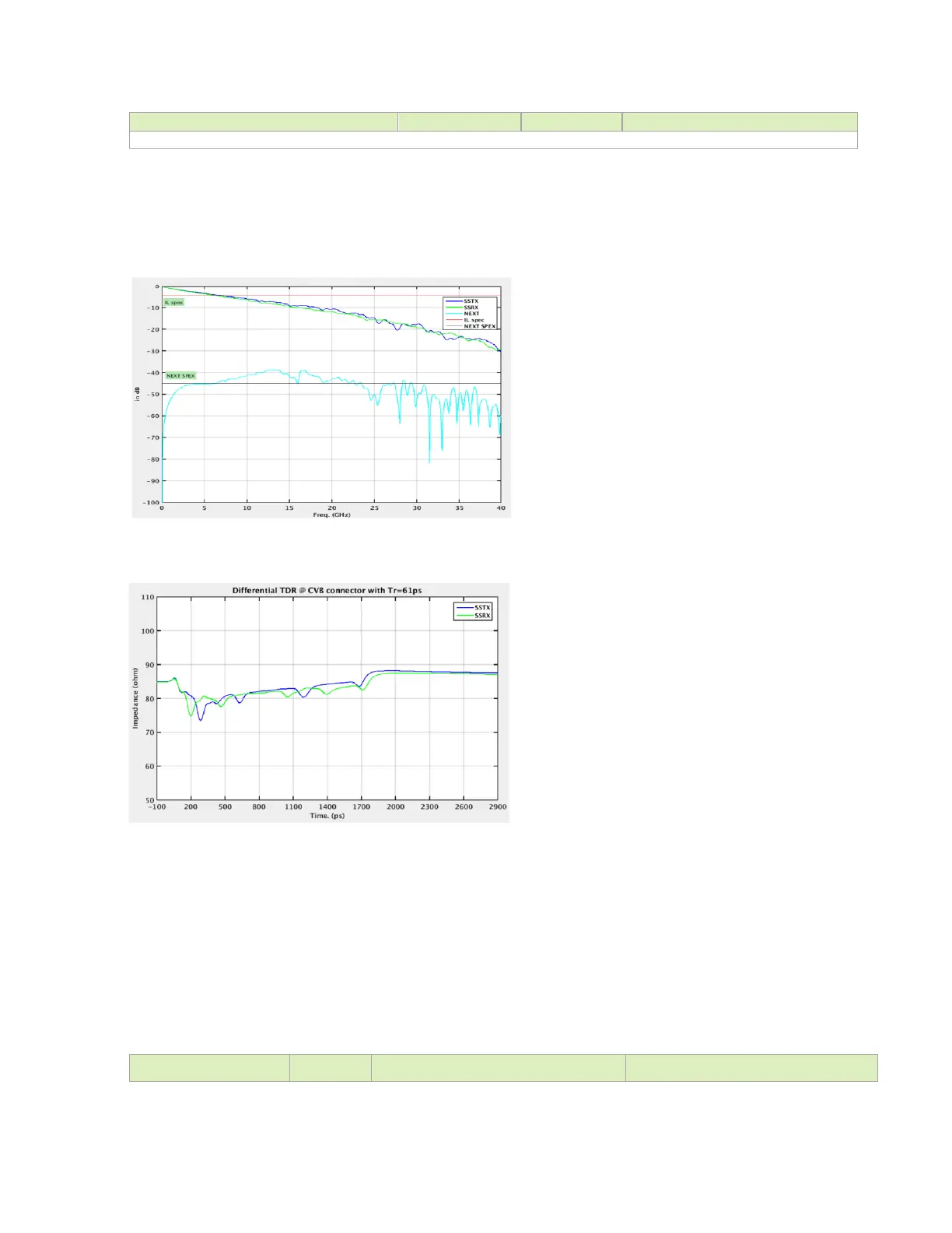
Figure 7-3. IL/NEXT Plot
Figure 7-4. TDR Plot
7.1.2.1 Common USB Routing Guidelines
If routing to USB device or USB connector includes a flex or 2nd PCB, the total routing
including all PCBs and flexes must be used for the max trace and skew calculations.
Keep critical USB related traces away from other signal traces or unrelated power traces and
areas or power supply components.
Table 7-7. Orin USB 2.0 Signal Connections
Module Ball Name
Type
Termination
Description

Table of Contents

Questions and Answers:

Question and Answer IconNeed help?

Do you have a question about the Nvidia Jetson Orin Nano Series and is the answer not in the manual?

Nvidia Jetson Orin Nano Series Specifications

General IconGeneral
BrandNvidia
ModelJetson Orin Nano Series
CategoryControl Unit
LanguageEnglish

Related product manuals