Miscellaneous Interfaces
PRELIMINARY INFORMATION
Jetson Orin NX Series and Jetson Orin Nano Series DG-10931-001_v1.1 | 74
Table 12-12. Orin Module Fan Pin Descriptions
Notes:
1. In the Direction column, Output is from Orin module. Input is to Orin module. Bidir is for Bidirectional signals.
2. The direction indicated for GPIO014 and GPIO08 is associated with their use as Fan PWM/Tach. The pins support GPIO
functionality, so support both input and output operation (bidirectional).
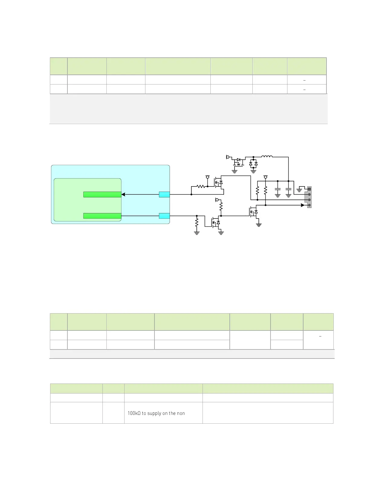
Figure 12-7. Orin Module Fan Connections
VDD_5V_IN
G
S
D
1
2
3
4
G
S
D
1k
10k
10uF
Fan
Header
Jetson
SoC Fan
GP31_PWM3
FAN_TACH
FAN_PWM
GP62
230
208
100k
GPIO08
GPIO14
VDD_5V_IN
G
S
D
10k
10k
VDD_1V8
G
S D
0.1uF
BAT54C
SM2309
PSAC-TRG
DMN26
DOUFB4
DMN26
DOUFB4
DMN26
DOUFB4
100uH
VDD_5V_IN
12.6 Debug
Orin Module supports a UART for debugging purposes. The UART intended for debug is
UART2.
Table 12-13. Orin Module Debug UART Pin Descriptions
Note: In the Direction column, Output is from Orin module. Input is to Orin module. Bidir is for Bidirectional signals.
Table 12-14. Debug UART Connections
UART #2 Transmit: Connect to RX pin of serial device
If level shifter implemented,
-Orin
module side of the device.
UART #2 Receive: Connect to TX pin of serial device
 Loading...