EasyManuals Logo
Home>Nvidia>Control Unit>Jetson Orin Nano Series

Nvidia Jetson Orin Nano Series User Manual

Nvidia Jetson Orin Nano Series
99 pages
To Next Page IconTo Next Page
To Previous Page IconTo Previous Page
Page #80 background imageLoading...
Page #80 background image
Miscellaneous Interfaces
PRELIMINARY INFORMATION
Jetson Orin NX Series and Jetson Orin Nano Series DG-10931-001_v1.1 | 69
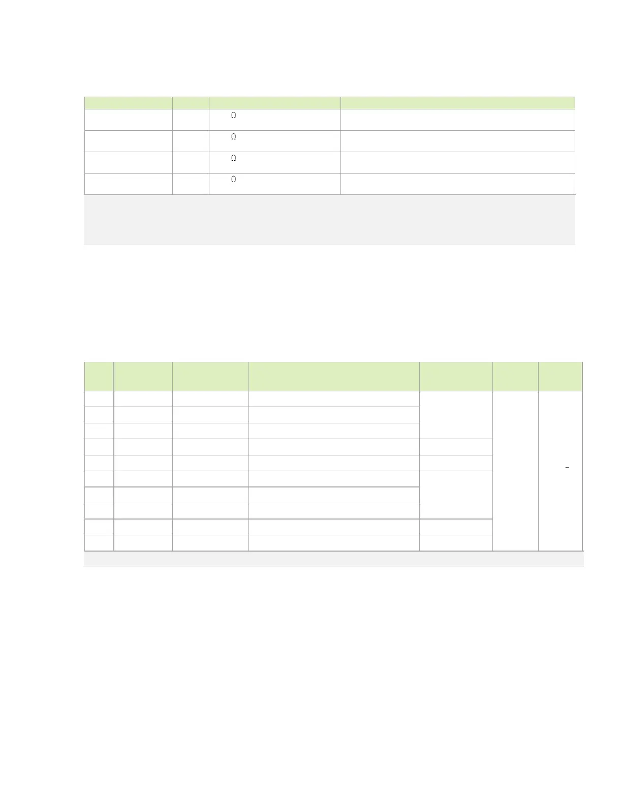
Table 12-3. I2C Signal Connections
Module Pin Name
Type
Termination
Description
I2C0_SCL/SDA
I/OD
1.5 k pull-ups to VDD_3V3 on
the module.
I2C #0 Clock and Data. Connect to CLK and Data pins of any
3.3V devices
I2C1_SCL/SDA
I/OD
2.2 k pull-ups to VDD_3V3 on
the module.
I2C #1 Clock and Data. Connect to CLK and Data pins of 3.3V
devices.
I2C2_SCL/SDA
I/OD
2.2 k pull-ups to VDD_1V8 on
the module.
I2C #2 Clock and Data. Connect to CLK and Data pins of any
1.8V devices
CAM_I2C_SCL/SDA
I/OD
2.2 k pull-ups to VDD_3V3 on
the module.
Camera I2C Clock and Data. Connect to CLK and Data pins
of any 3.3V devices
Notes:
1. If some devices require a different voltage level than others connected to the same I2C bus, level shifters are required.
2. For I2C interfaces that are pulled up to 1.8V, disable the RCV_33_18_SEL option for these pads. For I2C interfaces that are pulled
up to 3.3V, enable the RCV_33_18_SEL option. The RCV_33_18_SEL option is selected in the Pinmux registers.
12.2 SPI
The Orin module brings out two of the Orin SPI interfaces. See Figure 12-2.
Table 12-4. Orin Module SPI Pin Descriptions
Pin #
Module Pin
Name
Orin Signal
Usage and Description
Recommended
Usage
Direction
Pin Type
91
SPI0_SCK
GP47_SPI1_SCK
SPI 0 Clock
SPI #0 Device #0
or #1
Bidir
CMOS
1.8V
93
SPI0_MISO
GP48_SPI1_MISO
SPI 0 Initiator In / Target Out
89
SPI0_MOSI
GP49_SPI1_MOSI
SPI 0 Initiator Out / Target In
95
SPI0_CS0*
GP50_SPI1_CS0
SPI 0 Chip Select 0
SPI #0 Device #0
97
SPI0_CS1*
GP51_SPI1_CS1
SPI 0 Chip Select 1
SPI #0 Device #1
106
SPI1_SCK
GP36_SPI3_SCK
SPI 1 Clock
SPI #1 Device #0
or #1
108
SPI1_MISO
GP37_SPI3_MISO
SPI 1 Initiator In / Target Out
104
SPI1_MOSI
GP38_SPI3_MOSI
SPI 1 Initiator Out / Target In
110
SPI1_CS0*
GP39_SPI3_CS0
SPI 1 Chip Select 0
SPI #1 Device #0
112
SPI1_CS1*
GP40_SPI3_CS1
SPI 1 Chip Select 1
SPI #1 Device #1
Notes: In the Direction column, Output is from Orin module. Input is to Orin module. Bidir is for Bidirectional signals.

Table of Contents

Questions and Answers:

Question and Answer IconNeed help?

Do you have a question about the Nvidia Jetson Orin Nano Series and is the answer not in the manual?

Nvidia Jetson Orin Nano Series Specifications

General IconGeneral
BrandNvidia
ModelJetson Orin Nano Series
CategoryControl Unit
LanguageEnglish

Related product manuals