EasyManuals Logo
Home>Nvidia>Control Unit>Jetson Orin Nano Series

Nvidia Jetson Orin Nano Series User Manual

Nvidia Jetson Orin Nano Series
99 pages
To Next Page IconTo Next Page
To Previous Page IconTo Previous Page
Page #40 background imageLoading...
Page #40 background image
USB and PCIe
PRELIMINARY INFORMATION
Jetson Orin NX Series and Jetson Orin Nano Series DG-10931-001_v1.1 | 29
Pin
#
Module Pin
Name
Orin SoC Pin Name
(See Note 4)
Usage and Description
Recommended
Usage
Direction
Pin
Type
51
DP0_TXD2_N
HS_UPHY0_L2_RX_
N
USB 3.2 Receive (Port #2)
USB 3.2
connector,
device or hub
Input
USB 3.2
PHY
53
DP0_TXD2_P
HS_UPHY0_L2_RX_P
57
DP0_TXD3_N
HS_UPHY0_L2_TX_N
USB 3.2 Transmit (Port #2)
Output
USB 3.2
PHY
59
DP0_TXD3_P
HS_UPHY0_L2_TX_P
Notes:
1. In the Direction column, Output is from Orin module. Input is to Orin module. Bidir is for Bidirectional signals.
2. The direction shown in this table for GPxxx_PCIEx_RST* and GP185_PCIE_WAKE* signals is true when used for those PCIe
functions. Otherwise, if used as GPIOs, the direction is bidirectional.
3. The light blue highlighting for some of the module pins/functions is just to highlight the different functionality on those pins.
4. The table above shows Module Pin Names and Orin SoC Pin Names. For the Orin Module Function, which can be very different
than the Module Pin name, see the Pinout Matrix, full Pin Desc. xls attached to this document, or Table 7-3 below.
The following tables shows the supported UPHY mapping for the UPHY blocks [2,0]. The
mapping tables indicate which lanes of each UPHY block can be assigned for USB or PCIe.
Only one of the supported configurations per UPHY block can be used in a design. Each UPHY
block is programmed independently. It is not required to select the same configuration on
both UPHY blocks.
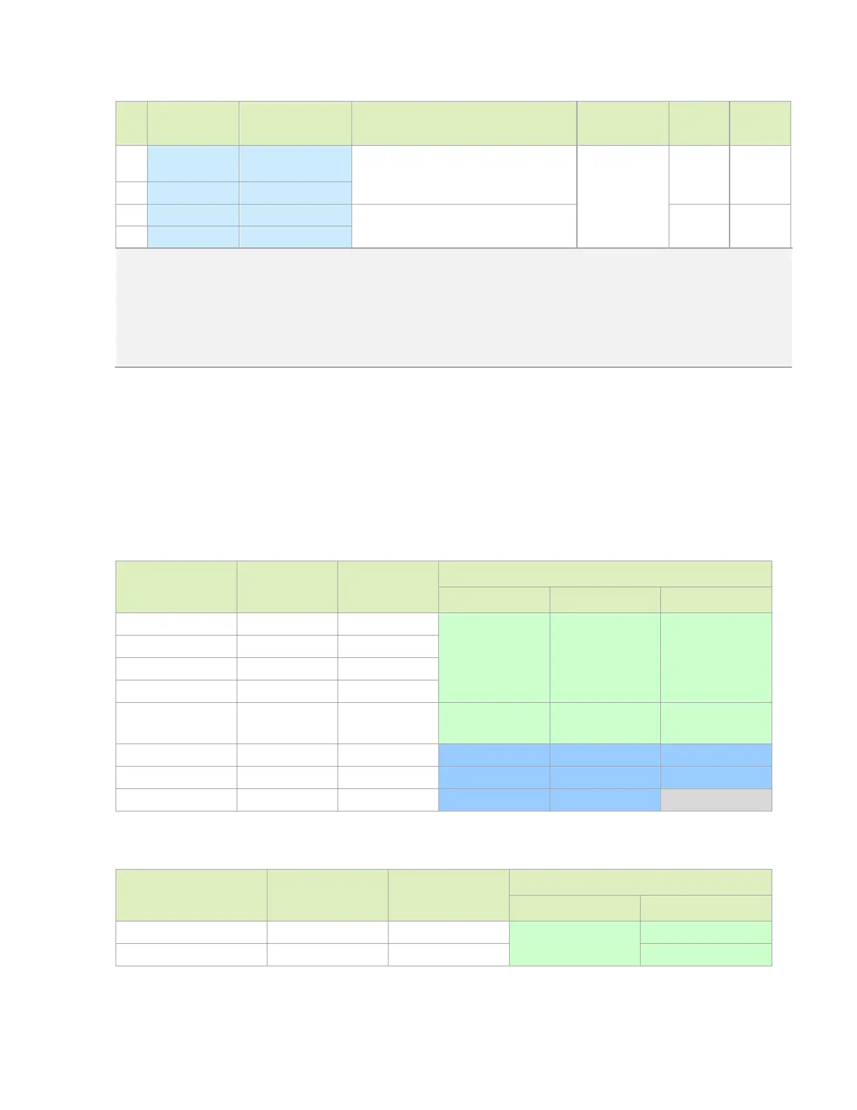
Table 7-3. UPHY0 Mapping Options (USB 3.2 and PCIe)
Orin Module Pin
Names
Orin Module
Functions
UPHY0 Lanes
Orin Module Configurations
Option #1
Option #2
Option #3
PCIE0_RX0/TX0
PCIe #0 Lane 0
UPHY0, Lane 4
PCIe x4 (C4), RP
PCIe x4 (C4), EP
PCIe x4 (C4), EP
PCIE0_RX1/TX1
PCIe #0 Lane 1
UPHY0, Lane 5
PCIE0_RX2/TX2
PCIe #0 Lane 2
UPHY0, Lane 6
PCIE0_RX3/TX3
PCIe #0 Lane 3
UPHY0, Lane 7
PCIE1_RX0/TX0
PCIe #1 Lane 0
UPHY0, Lane 3
PCIe x1 (C1), RP
PCIe x1 (C1), RP
Limited to Gen2
PCIe x1 (C1), RP
USBSS_RX/TX
USB 3.2 #1
UPHY0, Lane 0
USB 3.2 (P0)
USB 3.2 (P0)
USB 3.2 (P0)
DP0_TXD[1:0]_N/P
USB 3.2 #2
UPHY0, Lane 1
USB 3.2 (P1)
USB 3.2 (P1)
USB 3.2 (P1)
DP0_TXD[3:2]_N/P
USB 3.2 #3
UPHY0, Lane 2
USB 3.2 (P2)
USB 3.2 (P2)
Unused
Table 7-4. UPHY2 Mapping Options (PCIe)
Orin Module Pin
Names
Orin Module
Functions
UPHY2 Lanes
Orin Module Configurations
Option #1
Option #2
CSI4_D[0:2]_RX0/TX0
PCIe #2 Lane 0
Lane 0
PCIe x2 (C7), RP
PCIe x1 (C7), RP
CSI4_D[1:3]_RX1/TX1
PCIe #2 Lane 1
Lane 1
PCIe x1 (C9), RP

Table of Contents

Questions and Answers:

Question and Answer IconNeed help?

Do you have a question about the Nvidia Jetson Orin Nano Series and is the answer not in the manual?

Nvidia Jetson Orin Nano Series Specifications

General IconGeneral
BrandNvidia
ModelJetson Orin Nano Series
CategoryControl Unit
LanguageEnglish

Related product manuals