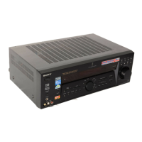
EasyManua.ls Logo

Sony STR-DE685 Service Manual

Sony STR-DE685
60 pages
To Next Page IconTo Next Page
To Previous Page IconTo Previous Page
Page #43 background imageLoading...
Page #43 background image
43
STR-DE685
The components identified by
mark 0 or dotted line with mark
0 are critical for safety.
Replace only with part number
specified.
Les composants identifiés par
une marque 0 sont critiques
pour la sécurité.
Ne les remplacer que par une
pièce portant le numéro spécifié.
153
151
154
152
T901
#2
#2
#3
#1
#1
#3
#1
F901
F902
not supplied
not supplied
not supplied
Q604
Q603
Q754
Q753
Q654
Q653
Q704
Q703
Q504
Q503
Ref. No. Part No. Description Remark Ref. No. Part No. Description Remark
151 A-4727-856-A STANDBY BOARD, COMPLETE (US,CND)
151 A-4727-868-A STANDBY BOARD, COMPLETE (AEP,UK,AUS)
151 A-4728-007-A STANDBY BOARD, COMPLETE (TW)
151 A-4728-008-A STANDBY BOARD, COMPLETE (MX)
151 A-4728-009-A STANDBY BOARD, COMPLETE (AR)
151 A-4728-017-A STANDBY BOARD, COMPLETE (KR)
151 A-4728-036-A STANDBY BOARD, COMPLETE (E,JE)
151 A-4728-040-A STANDBY BOARD, COMPLETE (SP,MY)
151 A-4728-044-A STANDBY BOARD, COMPLETE (CH)
152 A-4727-853-A MAIN BOARD, COMPLETE (US,CND)
152 A-4727-866-A MAIN BOARD, COMPLETE (AEP,UK,AUS)
152 A-4728-004-A MAIN BOARD, COMPLETE (TW)
152 A-4728-032-A MAIN BOARD, COMPLETE
(E,JE,MX,SP,MY,AR,KR)
152 A-4728-043-A MAIN BOARD, COMPLETE (CH)
153 3-905-609-01 SCREW (TRANSISTOR)
154 3-701-946-27 LABEL, FUSE RATING (US,CND,MX,TW)
0 F901 1-532-464-31 FUSE, TIME-LAG (T2.5AL/250V)
(EXCEPT US,CND,MX,TW)
0 F901 1-576-193-11 FUSE (6.3A/125V) (US,CND,MX,TW)
0 F902 1-532-464-31 FUSE, TIME-LAG (T2.5AL/250V)
(AEP,UK,AUS,SP,MY)
0 F902 1-576-109-11 FUSE (5A/125V) (US,CND)
Q503 8-749-010-25 TRANSISTOR MN2488-OPY-M
Q504 8-749-010-26 TRANSISTOR MP1620-OPY-M
Q603 8-749-010-25 TRANSISTOR MN2488-OPY-M
Q604 8-749-010-26 TRANSISTOR MP1620-OPY-M
Q653 8-749-010-25 TRANSISTOR MN2488-OPY-M
Q654 8-749-010-26 TRANSISTOR MP1620-OPY-M
Q703 8-749-010-25 TRANSISTOR MN2488-OPY-M
Q704 8-749-010-26 TRANSISTOR MP1620-OPY-M
Q753 8-749-010-25 TRANSISTOR MN2488-OPY-M
Q754 8-749-010-26 TRANSISTOR MP1620-OPY-M
0 T901 1-435-899-11 TRANSFORMER, POWER (TW)
0 T901 1-435-901-11 TRANSFORMER, POWER (E,JE)
0 T901 1-435-903-11 TRANSFORMER, POWER
(AEP,UK,AUS,CH,SP,MY,AR,KR)
0 T901 1-435-905-11 TRANSFORMER, POWER (CND)
0 T901 1-435-906-11 TRANSFORMER, POWER (MX)
0 T901 1-437-699-11 TRANSFORMER, POWER (US)
#1 7-685-646-79 SCREW +BVTP 3X8 TYPE2 IT-3
#2 7-685-880-09 SCREW +BVTT 4X6 (S)
#3 7-685-645-79 SCREW +BVTP 3X6 TYPE2 N-S
5-4. CHASSIS SECTION-2
Ver 1.1

Other manuals for Sony STR-DE685

Question and Answer IconNeed help?

Do you have a question about the Sony STR-DE685 and is the answer not in the manual?
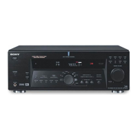
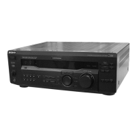
Sony STR-DE685 Specifications

General IconGeneral
Channels5.1
Total Harmonic Distortion0.09%
Power Output100 W per channel (8 ohms, 20 Hz - 20 kHz, 0.09% THD)
Tuning rangeAM/FM
Frequency response10 Hz - 100 kHz
Speaker load impedance8 ohms
Digital inputs1 x Optical, 1 x Coaxial
Video ConnectionsComposite video inputs

Summary

Audio Power Specifications

Power Output and Total Harmonic Distortion

Specifies RMS power output and total harmonic distortion for minimum power.

Amplifier Section Power Output

Details rated power output for stereo mode across different area codes.

Specifications Overview

Tuner Section Specifications

Safety Information

Safety Check-out and Leakage Test

Details safety checks, including AC leakage testing procedures and limits.

Safety-Related Component Warnings

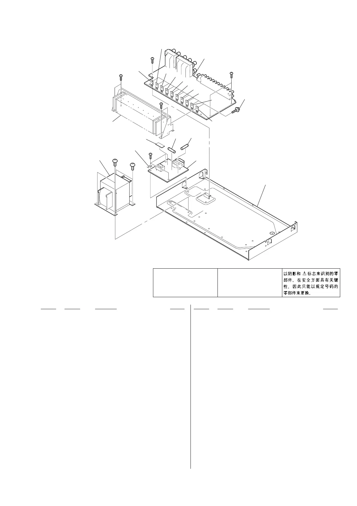
Highlights critical components that are essential for safe operation.

Remote Control Operation

Disassembly Procedures

Test Modes

Diagrams

IC Pin Descriptions (IC1201 DSP) Part 1/2

Lists pin functions and descriptions for the DSP IC (part 1/2).

IC1201 Pin Descriptions (DSP) Part 2/2

Continues pin functions and descriptions for the DSP IC.

IC1601 Pin Descriptions (System Control) Part 1/2

Lists pin functions and descriptions for the System Control IC (part 1/2).

IC1601 Pin Descriptions (System Control) Part 2/2

Continues pin functions and descriptions for the System Control IC.

Block Diagrams

Tuner/Audio Section Block Diagram

Illustrates the signal flow within the tuner and audio processing sections.

Digital Section Block Diagram

Shows the signal paths and interconnections within the digital processing circuitry.

Key/Display Section Block Diagram

Illustrates the operation of the front panel controls and display elements.

Video Section Block Diagram

Depicts the signal flow and processing for video inputs and outputs.

Power Section Block Diagram

Shows the power supply distribution and regulation circuitry.

Circuit Boards Location and Waveforms

Circuit Diagrams and Layouts

Main Board Schematics and PWB

Provides printed wiring board layout and schematic diagrams for the main board.

Digital Board Schematics and PWB

Shows printed wiring boards and schematics for the digital section (parts 1 & 2).

Display Board Schematics and PWB

Presents printed wiring boards and schematics for the display section.

Video and S-Video Sections Schematics and PWB

Covers printed wiring boards and schematics for video, S-Video, and Speaker B sections.

Power Section Schematics and PWB

Provides printed wiring boards and schematics for the power supply section.

IC Block Diagrams

IC301/IC302 Component Video Board Diagrams

Block diagrams and pinouts for IC301 (multiplexer) and IC302 (amplifier) on the component video board.

Exploded Views

Electrical Parts List

Related product manuals