2-24
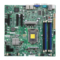
X10DRL-i Motherboard User’s Manual
Power Button
OH/Fan Fail/
PWR Fail LED)
1
NIC1 Link LED
Reset Button
2
Power Fail LED
HDD LED
FP PWRLED
Reset
PWR
3.3 V
UID Switch
UID LED
Ground
Ground
1920
3.3V
X
Ground
NMI
X
NIC2 Link LED
NIC2 Activity LED
NIC1 Activity LED
Power Button
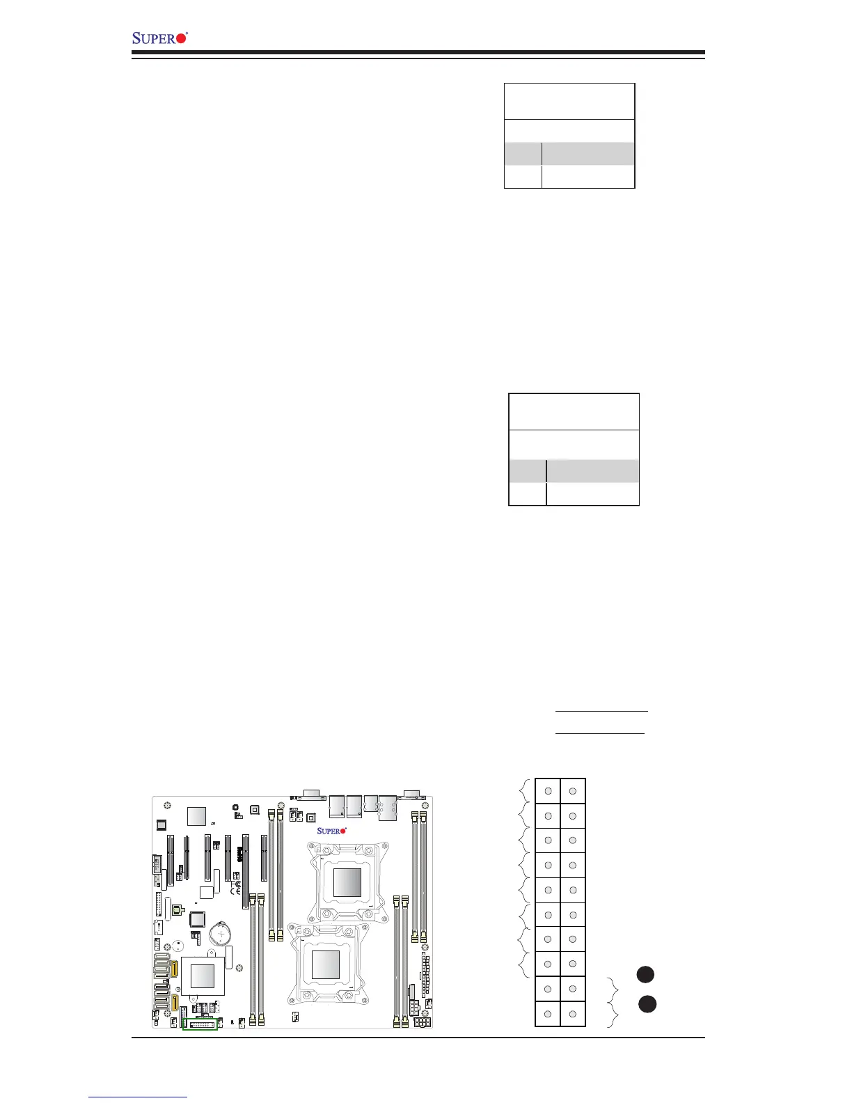
The Power Button connection is located
on pins 1 and 2 of JF1. Momentarily
contacting both pins will power on/off
the system. This button can also be con-
gured to function as a suspend button
(with a setting in the BIOS - See Chapter
4). To turn off the power when the system
is in suspend mode, press the button for
4 seconds or longer. Refer to the table on
the right for pin denitions.
Power Button
Pin Denitions (JF1)
Pin# Denition
1 Signal
2 Ground
Reset Button
The Reset Button connection is located
on pins 3 and 4 of JF1. Attach it to a
hardware reset switch on the computer
case. Refer to the table on the right for
pin denitions.
Reset Button
Pin Denitions (JF1)
Pin# Denition
3 Reset
4 Ground
A. Reset Button
B. PWR Button
A
B
LE6
JBT1
BIOS
LICENSE
JPI2C1
J24
JPWR2
JF1
JD1
JL1
JSD1
BT1
JTPM1
JPL1
JPL2
JPG1
JPB1
JWD1
JI2C2
JPME2
JI2C1
JPF1
JPF2
J23
SP1
JUIDB1
LE2
LE1
LEDM1
FANB
FAN4
FAN3
FAN1
FAN5
FAN6
FANA
MAC CODE
BAR CODE
(3.0)
USB12/13
USB2/3
USB4
USB0/1
JSTBY1
JIPMB1
S-SATA2
S-SATA0
COM2
S-SATA1
S-SATA3
I-SATA5
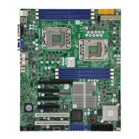
PCH SLOT1 PCI-E 2.0
X4(IN X8)
I-SATA4
CPU1 SLOT2 PCI-E 3.0 X8
I-SATA3
I-SATA2
I-SATA1
CPU1 SLOT3 PCI-E 3.0 X8
I-SATA0
CPU2 SLOT4 PCI-E 3.0 X4 (IN X8)
CPU1 SLOT5 PCI-E 3.0 X16
CPU1 SLOT6 PCI-E 3.0 X8
UID
P2-DIMME1
P1-DIMMC1
P2-DIMMF1
P1-DIMMD1
P2-DIMMH1
P1-DIMMB1
VGA
P1-DIMMA1
CPU1
LAN2
P2-DIMMG1
CPU2
LAN1
IPMI_LAN
COM1
JPWR1
BMC
PCH
LAN CTRL
LAN CTRL
CLOSE 1st
OPEN 1st
CLOSE 1st
OPEN 1st
USB8/9(3.0)
BIOS
I-SGPIO1
S-SGPIO
1
J10
FAN2
X10DRL-i
Rev. 1.01
I-SGPIO2
IPMI CODE
 Loading...