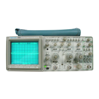
Theory of Operation—2215A Service
When the instrument is first turned on, one of the switch
ing transistors will start to conduct and its collector voltage
will drop toward the common voltage level. This will induce a
positive voltage from the lead of T944 which is connected to
the base of the conducting transistor and reinforce conduc
tion. Eventually T944 will saturate, and as the voltage
across T944 (and T948) begins to reverse, the conducting
transistor will cut off because of the drop in base drive. The
other transistor will not start conduction until the voltage on
the leads of T944 reverse enough to bias it on. This process
will continue, and the saturation time of T944 plus the tran
sistor-switching time will determine the frequency of Inverter
operation (typically 20 kHz). After the initial Inverter start up,
the switching transistors do not saturate; they remain in the
active region during switching.
Diodes CR946 and CR947 serve as a negative-peak de
tector to generate a voltage for controlling the output of the
error amplifier. Capacitor C943 charges to a voltage equal
to the negative peak voltage at the collectors of Q946 and
Q947, referenced to the Preregulator input voltage. This
voltage level is applied to the divider composed of R937,
R938, and R939. The error amplifier, composed of Q938
and Q939, is a differential amplifier that compares the refer
ence voltage of VR943 with the voltage on the wiper of
potentiometer R938. The current through Q939 will set the
base drive of Q944 and thereby control the voltage on
C944. This voltage will bias Q946 and Q947 to a level that
will maintain the peak-to-peak input voltage of T948. The
amplitude of the voltage across the transformer primary
winding, and thus that of the secondary voltages of T948, is
set by adjusting —8.6 V Adj potentiometer R938.
At turn on, Q938 is biased off and Q939 is biased on. All
the current of the error amplifier will then go through Q939
to bias on Q944. Diode CR945 allows the base of Q944 to
go positive enough to initially turn on Q946 or Q947. The
current through Q944 controls the base drive for Q946 and
Q947. Base current provided by base-drive transformer
T944 will charge C944 negative with respect to the Inverter
circuit floating ground (common) level.
Crt Supply
High-voltage multiplier U975 utilizes the 2-kV winding of
T948 to generate 12 kV to drive the crt anode. It also uses
an internal half-wave rectifier diode to produce — 2 kV for
the crt cathode. The — 2 kV supply is filtered by a low-pass
filter composed of C975, C976, R976, R978, and C979.
Neon lamp DS870 protects against excessive voltage be
tween the crt heater and crt cathode by conducting if the
voltage exceeds approximately 75 V.
Focus Circuit
Focus voltage is also developed from the — 2 kV supply
via a voltage divider composed of R894, R892, FOCUS
potentiometer R893, R891, R890, R889, R888, and Q885.
The focus voltage tracks the A-intensity level through the
action of Q885. The emitter voltage of Q804, set by the A
INTENSITY control, is applied to the emitter of Q885
through R885. When the emitter voltage of Q804 changes,
the current through Q885 changes proportionally and alters
the voltage at one end of FOCUS control R893.
Low-Voltage Supplies
The low-voltage supplies utilize center-tapped secondary
windings of T948. The +100 V supply uses CR954 and
CR955 for rectification and C954 for filtering. Diodes CR956
and CR957 rectify ac from taps on the 100 V winding, and
C956 filters the output to produce +30 V dc. The diode
bridge consisting of CR960, CR961, CR962, and CR963
produces the +8.6 V and -8 .6 V supplies. Filtering of the
+ 8.6 V is accomplished by C960, C962, and L960; filtering
of the —8.6 V is done by C961, C963, and L961. The +5.2
V supply is produced by CR967, CR970, C968, R971, and
C970.
Probe Adjust
The Probe Adjust circuitry, shown on diagram 6, utilizes
a square-wave generator and a diode switching network to
produce a negative-going square-wave signal at PROBE
ADJUST connector J9900. Amplifier U985 is configured as
a multivibrator with the time constant of R987 and C987
determining the oscillation period. When the output of the
multivibrator is at the positive supply voltage, CR988 is for
ward biased. This reverse biases CR989 and the PROBE
ADJUST connector signal is held at ground potential by
R990. When the multivibrator output switches states and is
at the negative supply voltage, CR988 is reverse biased.
Diode CR989 will now be forward biased and the circuit
output signal be approximately —0.5 V.
3-18

 Loading...