(2) The UART switch path connects from the UART buffers to the port pins. See Section 7.19 for buffer specifications.
(3) See Section 7.16 for the USB_EP specifications.
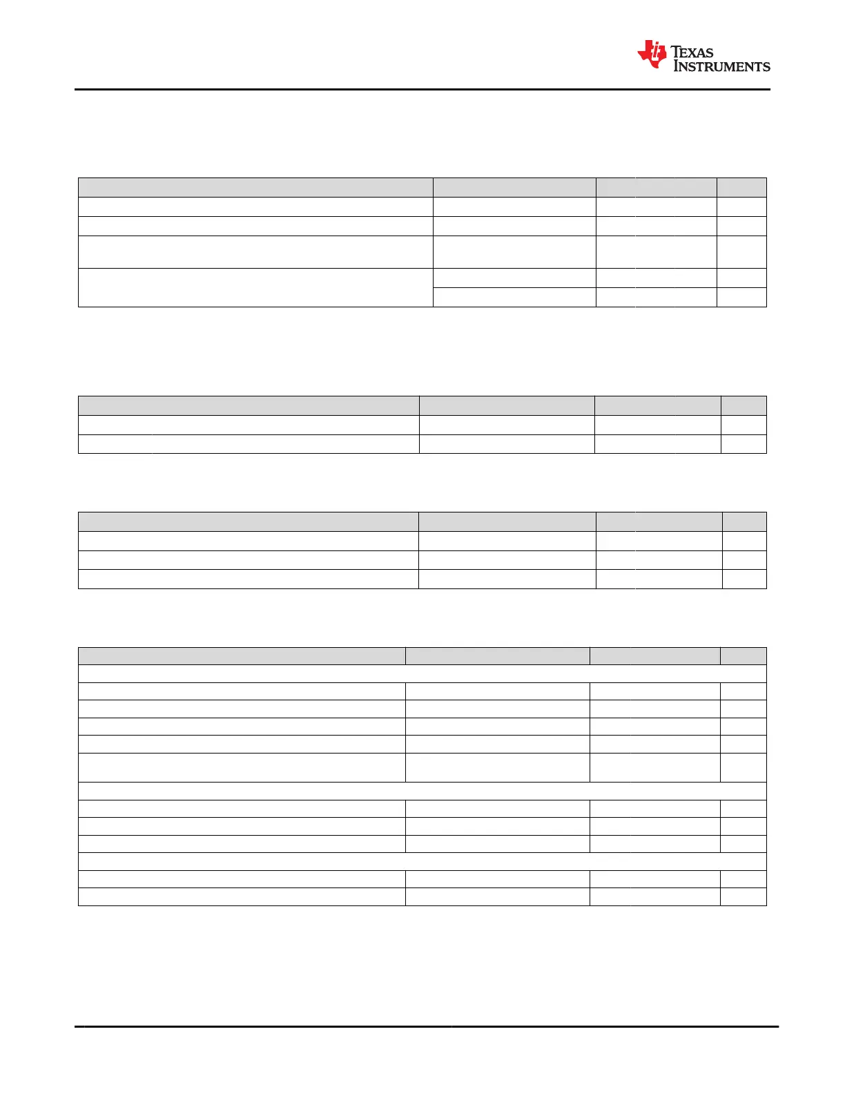
7.13 Port Data Multiplexer Clamp Characteristics
Recommended operating conditions; T
A
= –10 to 85°C unless otherwise noted
PARAMETER TEST CONDITIONS MIN TYP MAX UNIT
VCLMP_IND Clamp voltage triggering indicator to digital core 3.8 3.95 4.1 V
ICLMP_IND Clamp current at VCLMP_IND 10 250 μA
TCLMP_PRT
(1)
Time from clamp current crossing ICLMP_IND to
interrupt signal assertion
I ≥ ICLMP_IND rising 0 4 μs
ICLMP USB_EP and USB_RP port clamp current
V = LDO_3V3 250 nA
V = VCLMP_IND + 500 mV 3.5 15 mA
(1) The TCLMP_PRT time includes the time through the digital synchronizers. When the clock speed is reduced, the signal assertion time
may be longer.
7.14 Port Data Multiplexer SBU Detection Characteristics
Recommended operating conditions; T
A
= –10 to 85°C unless otherwise noted
PARAMETER TEST CONDITIONS MIN TYP MAX UNIT
VIH_PORT Port switch detect input high voltage LDO_3V3 = 3.3 V 2 v
VIL_PORT Port switch detect input low voltage LDO_3V3 = 3.3 V 0.8 V
7.15 Port Data Multiplexer Signal Monitoring Pullup and Pulldown Characteristics
Recommended operating conditions; T
A
= –10 to 85°C unless otherwise noted
PARAMETER TEST CONDITIONS MIN TYP MAX UNIT
RPU05 500-Ω pullup and pulldown resistance LDO_3V3 = 3.3 V 350 500 650 Ω
RTPU5 5-kΩ pullup and pulldown resistance LDO_3V3 = 3.3 V 3.5 5 6.5 kΩ
RPU100 100-kΩ pullup and pulldown resistance LDO_3V3 = 3.3 V 70 100 130 kΩ
7.16 Port Data Multiplexer USB Endpoint Characteristics
Recommended operating conditions; T
A
= –10 to 85°C unless otherwise noted
PARAMETER TEST CONDITIONS MIN TYP MAX UNIT
TRANSMITTER
(1)
T_RISE_EP Rising transition time Low-speed (1.5 Mbps) data rate only 75 300 ns
T_FALL_EP Falling transition time Low-speed (1.5 Mbps) data rate only 75 300 ns
T_RRM_EP Rise/fall time matching Low-speed (1.5 Mbps) data rate only –20% 25%
V_XOVER_EP Output crossover voltage 1.3 2 V
RS_EP Source resistance of driver including 2nd stage port
data multiplexer
34
Ω
DIFFERENTIAL RECEIVER
(1)
VOS_DIFF_EP Input offset –100 100 mV
VIN_CM_EP Common mode range 0.8 2.5 V
RPU_EP D– Bias Resistance Receiving 1.425 1.575 kΩ
SINGLE ENDED RECEIVER
(1)
VTH_SE_EP Single ended threshold Signal rising and falling 0.8 2 V
VHYS_SE_EP Single ended threshold hysteresis Signal falling 200 mV
(1) The USB Endpoint PHY is functional across the entire VIN_3V3 operating range, but parameter values are only verified by design for
VIN_3V3 ≥ 3.135 V
TPS65982
SLVSD02E – MARCH 2015 – REVISED AUGUST 2021
www.ti.com
22 Submit Document Feedback
Copyright © 2021 Texas Instruments Incorporated
Product Folder Links: TPS65982

 Loading...