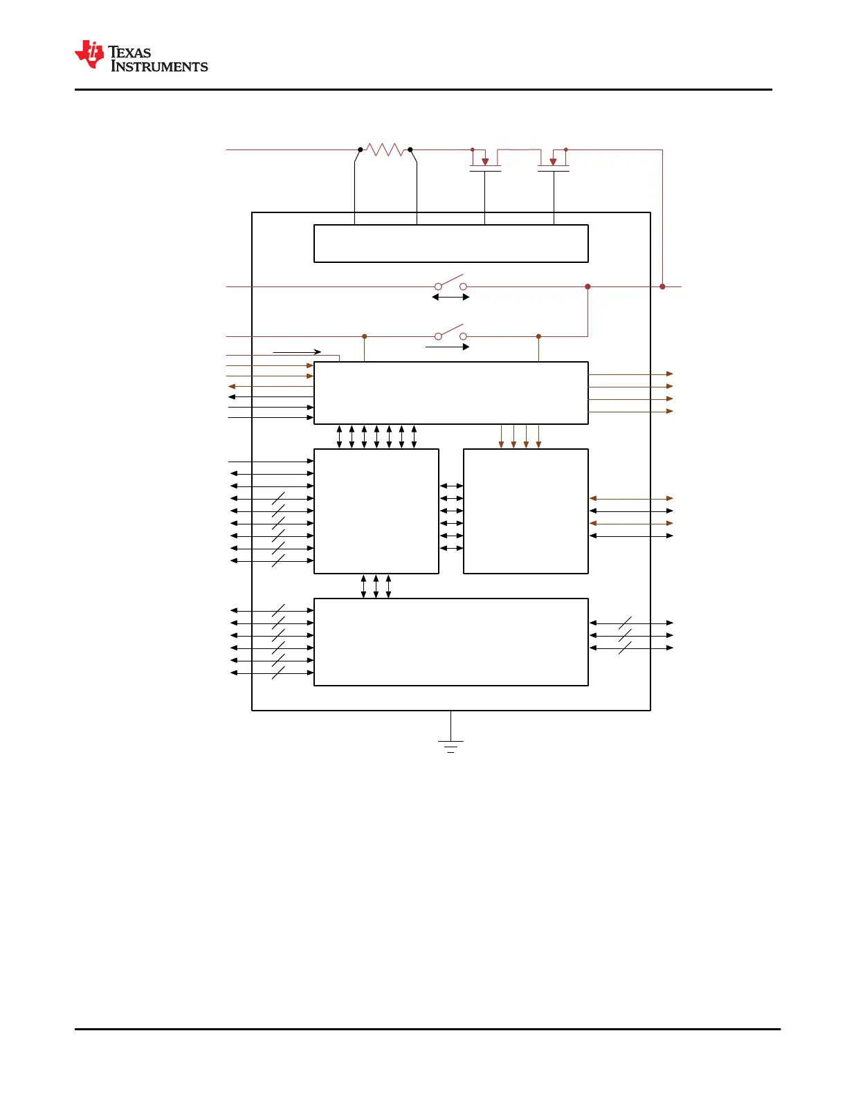
9.2 Functional Block Diagram
Digital Core
Power Management and Supervisors
Port Data Multiplexer
NMOS
External FET Control and Sense
2
2
2
2
2
2
3
3
4
2
9
2
2
2
C_USB_TP/TN
C_USB_BP/BN
C_SBU1/2
C_CC1
C_CC2
VBUS
PP_5V0
VIN_3V3
RESETZ
MRESET
HRESET
VOUT_3V3
LDO_3V3
LDO_1V8A
LDO_1V8D
LDO_BMC
BUSPOWERZ
R_OSC
GPIO1-9
I2C_SDA/SCL/IRQ1Z
I2C_SDA/SCL/IRQ2Z
SPI_PICO/POCI/CSZ/CLK
SWD_DATA/CLK
I2C_ADDR
PP_HV
PP_CABLE 3 A
3 A
600 mA
SENSEP SENSEN
GND
2
DEBUG_CTL1/2
UART_RX/TX
LSX_R2P/P2R
AUX_P/N
USB_RP_P/N
DEBUG1/2
DEBUG3/4
RPD_G1
RPD_G2
PP_EXT
HV_GATE1 HV_GATE2
VDDIO
Cable/Device
Detect,
and
USB-PD Phy
Cable Power,
9.3 Feature Description
9.3.1 USB-PD Physical Layer
Figure 9-1 shows the USB PD physical layer block surrounded by a simplified version of the analog plug and
orientation detection block.
www.ti.com
TPS65982
SLVSD02E – MARCH 2015 – REVISED AUGUST 2021
Copyright © 2021 Texas Instruments Incorporated
Submit Document Feedback
33
Product Folder Links: TPS65982

 Loading...