10 Application and Implementation
Note
Information in the following applications sections is not part of the TI component specification,
and TI does not warrant its accuracy or completeness. TI’s customers are responsible for
determining suitability of components for their purposes, as well as validating and testing their design
implementation to confirm system functionality.
10.1 Application Information
The typical applications of the TPS65982 include chargers, notebooks, tablets, ultrabooks, docking systems,
dongles, and any other product supporting USB Type-C, USB-PD as a power source, power sink, data DFP,
data UFP, or dual-role port (DRP), or supporting both USB Type-C andUSB-PD. The typical applications outlined
in the following sections detail a Fully-Featured USB Type-C and PD Charger Application and a Dual-Port
Notebook Application Supporting USB PD Charging and DisplayPort.
10.2 Typical Applications
10.2.1 Fully-Featured USB Type-C and PD Charger Application
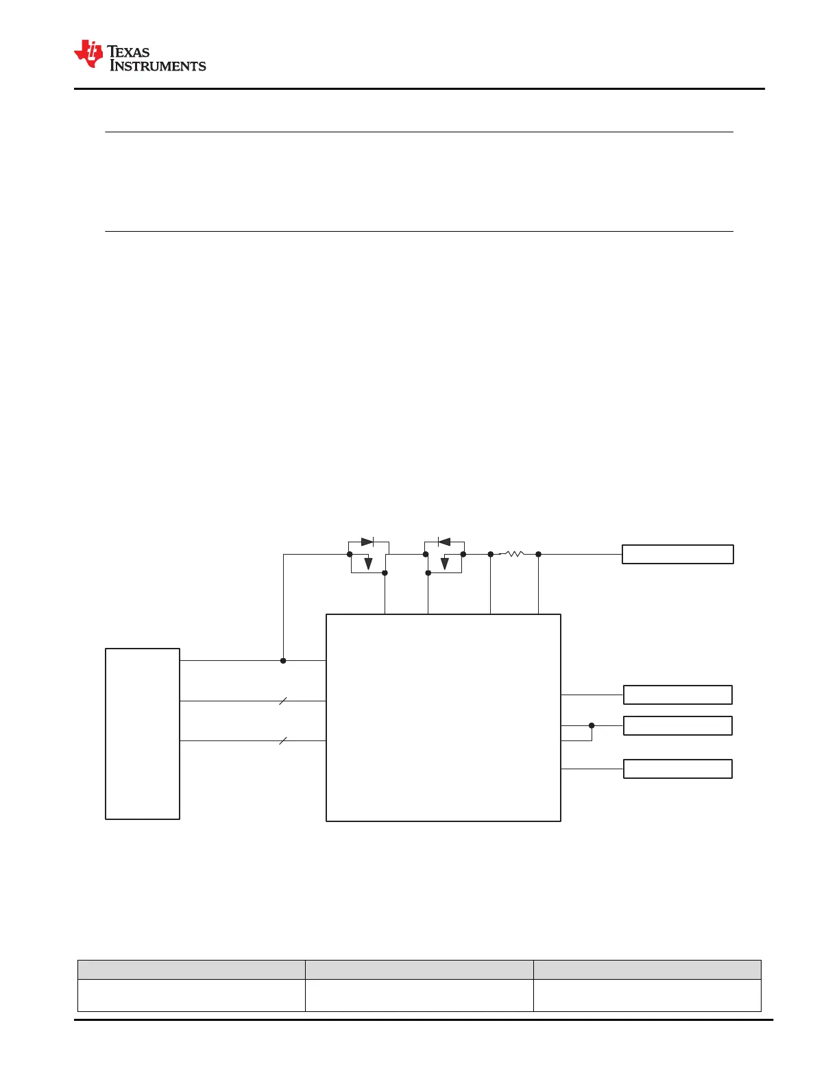
The TPS65982 controls three separate power paths making it a flexible option for Type C PD charger
applications. In addition, the TPS65982 supports VCONN power for e-marked cables which are required for
applications which require greater than 3 A of current on VBUS. Figure 10-1 below shows the high level block
diagram of a Type C PD charger that is capable of supporting 5 V at 3 A, 12 V at 3 A, and 20 V at 5 A. The 5
V and 12 V outputs are supported by the TPS65982 internal FETs and the 20-V output uses the external FET
path controlled by the TPS65982 NFET drive. This Type-C PD charger uses a receptacle for flexibility on cable
choice.
VBUS
CC1/2
SSTX/RX
SBU1/2
USB2.0
Type C
Receptacle
TPS65982
(Charger Application)
VBUS
CC1/2
HV_GATE1
USB2.0
HV_GATE2
SENSEN
SENSEP
PP_HV
PP_5V0
VIN_3V3
PP_CABLE
Supply 20 V, 5 A
Supply 12 V, 3 A
Supply 5 V, 3.5 A
Supply 3.3 V, 50 mA
Copyright © 2016, Texas Instruments Incorporated
Figure 10-1. Type-C and PD Charger Application
10.2.1.1 Design Requirements
For a USB Type-C and PD Charger application, Table 10-1 lists the input voltage requirements and expected
current capabilities.
Table 10-1. Charging Application Design Parameters
DESIGN PARAMETER EXAMPLE VALUE DIRECTION OF CURRENT
PP_5V0 Input Voltage and Current
Capabilities
5 V, 3 A Sourcing to VBUS
www.ti.com
TPS65982
SLVSD02E – MARCH 2015 – REVISED AUGUST 2021
Copyright © 2021 Texas Instruments Incorporated
Submit Document Feedback
81
Product Folder Links: TPS65982

 Loading...