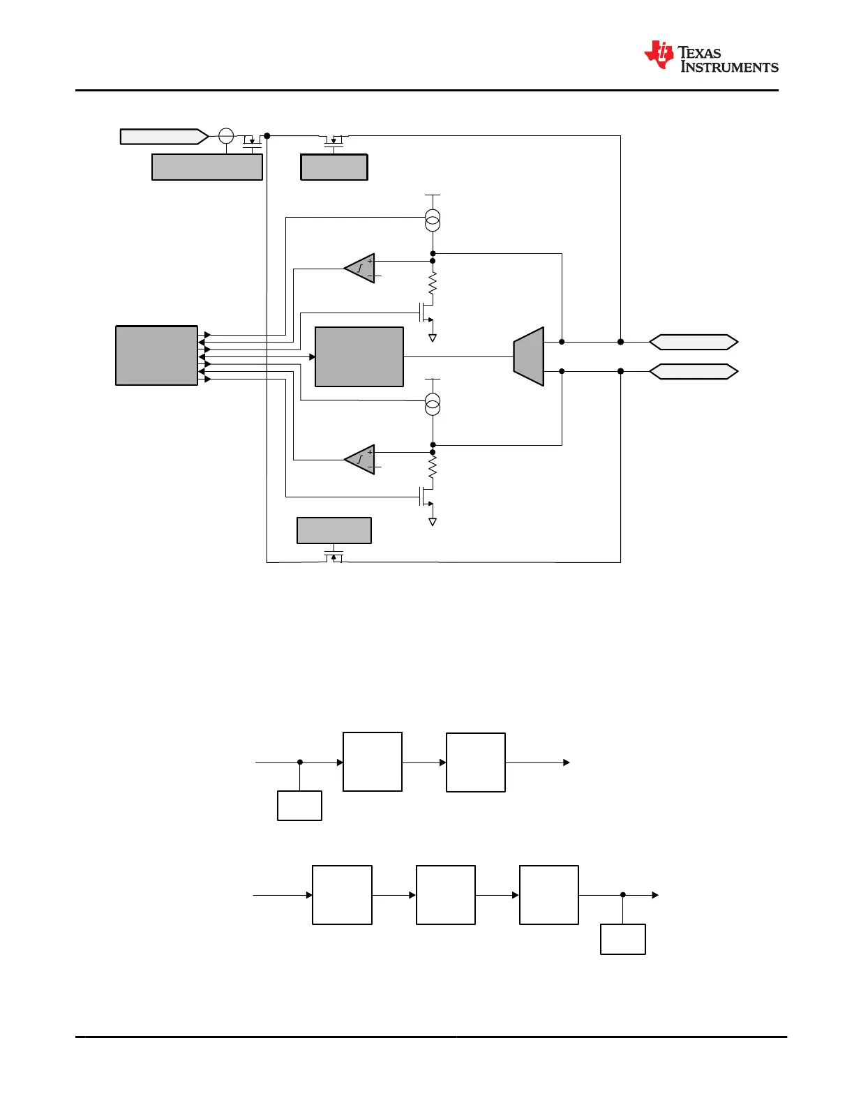
USB-PD
Digital Core
Phy
LDO_3V3
LDO_3V3
C_CC2
C_CC1
PP_CABLE
C_CC1/2 Gate Control
and Current Limit
C_CC1 Gate
Control
Fast
current
limit
C_CC2 Gate
Control
Figure 9-1. USB-PD Physical Layer and Simplified Plug and Orientation Detection Circuitry
USB-PD messages are transmitted in a USB Type-C system using a BMC signaling. The BMC signal is output
on the same pin (C_CC1 or C_CC2) that is DC biased because of the DFP (or UFP) cable attach mechanism
discussed in the Cable Plug and Orientation Detection section.
9.3.1.1 USB-PD Encoding and Signaling
Figure 9-2 shows the high-level block diagram of the baseband USB-PD transmitter. Figure 9-3 shows the
high-level block diagram of the baseband USB-PD receiver.
4b5b
Encoder
BMC
Encoder
CRC
Data
to PD_TX
Figure 9-2. USB-PD Baseband Transmitter Block Diagram
BMC
Decoder
SOP
Detect
4b5b
Decoder
CRC
from PD_RX
Data
Figure 9-3. USB-PD Baseband Receiver Block Diagram
TPS65982
SLVSD02E – MARCH 2015 – REVISED AUGUST 2021
www.ti.com
34 Submit Document Feedback
Copyright © 2021 Texas Instruments Incorporated
Product Folder Links: TPS65982

 Loading...