SARA-R4/N4 series - System Integration Manual
UBX-16029218 - R11 Design-in Page 107 of 157
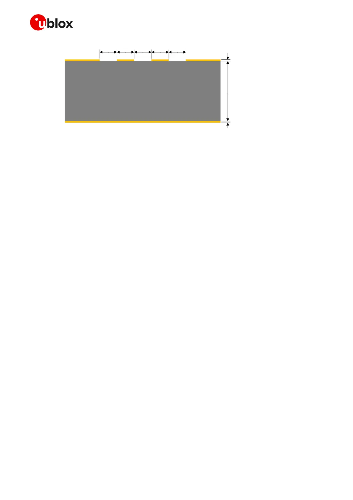
35 µm
35 µm
1510 µm
L2 Copper
L1 Copper
FR-4 dielectric
740 µm 410 µm410 µm740 µm410 µm
Figure 50: Example of USB line design, with Z
0
close to 90 and Z
CM
close to 30 , for the described 2-layer board layup
2.6.3 SPI interface
2.6.3.1 Guidelines for SPI circuit design
☞ The SPI interface is not supported by “00”, “01”, “02” and “52” product versions: the SPI interface pins
should not be driven by any external device.
2.6.4 SDIO interface
2.6.4.1 Guidelines for SDIO circuit design
☞ The SDIO interface is not supported by “00”, “01”, “02” and “52” product versions: the SDIO interface
pins should not be driven by any external device.
2.6.5 DDC (I
2
C) interface
2.6.5.1 Guidelines for DDC (I
2
C) circuit design
☞ DDC (I
2
C) interface is not supported by “00” and “01” product versions: the DDC (I
2
C) interface pins
should not be driven by any external device.
The DDC I
2
C-bus master interface can be used to communicate with u-blox GNSS receivers and other
external I
2
C-bus slaves as an audio codec.
The SDA and SCL pins of the module are open drain output as per I
2
C bus specifications [9], and they have
internal pull-up resistors to the V_INT 1.8 V supply rail of the module, so there is no need of additional
pull-up resistors on the external application board.
 Loading...


