
Do you have a question about the Xilinx ML605 and is the answer not in the manual?
| Form Factor | ATX |
|---|---|
| DDR3 SODIMM | 1GB |
| Flash Memory | 128MB |
| Ethernet | 10/100/1000 Mbps |
| USB | USB 2.0 |
| Clocking | 200 MHz oscillator |
| USB Ports | 1 |
| Ethernet Ports | 1 |
| FPGA Device | Xilinx Virtex-6 LX240T |
| Memory | DDR3 |
| PCI Express | x8 |
| Connectors | FMC |
| Expansion Slots | FMC |
| Power Connector | ATX |
| Operating Temperature | 0°C to 55°C |
| Power Supply | ATX |
Lists related Xilinx documents for download.
Details on how to find technical support via the Xilinx website.
Introduces the ML605 board and its target FPGA.
Lists the key hardware features and components of the ML605 board.
Shows a high-level block diagram of the ML605 board and its peripherals.
Lists related Xilinx documents and resources for additional information.
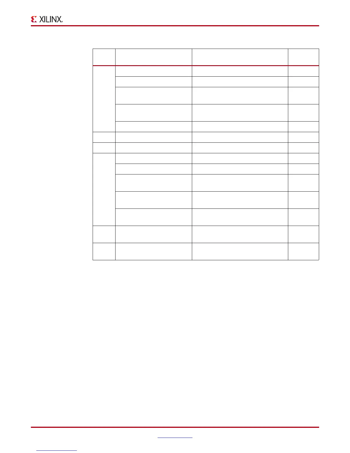
Provides detailed descriptions of the ML605 board's components and features.
Details the main FPGA chip installed on the ML605 board.
Details the voltage rails supplied to the FPGA I/O banks on the ML605 board.
Describes the 512MB DDR3 SODIMM memory module and its connections.
Details the 128Mb Platform Flash XL device used for FPGA configuration.
Details the 32MB Linear BPI Flash memory used for configuration and storage.
Explains how to select between Platform Flash and BPI Flash for boot.
Describes the System ACE CF controller and CompactFlash card interface.
Explains the USB JTAG interface for configuration and debugging.
Details the three FPGA fabric clock sources available on the ML605.
Describes the 20 MGTs available on the ML605 and their connectivity.
Details the PCIe x8 edge connector and its connectivity for Gen1 and Gen2.
Describes the SFP connector for network modules and its control signals.
Details the Marvell Alaska PHY for Ethernet communications at various speeds.
Describes the clock generation for the SGMII GTX transceiver.
Explains the Silicon Labs CP2103GM USB-to-UART bridge for serial communication.
Details the Cypress CY7C67300 USB Host and Peripheral Controller.
Describes the Chrontel CH7301C DVI connector for video output.
Details the four IIC bus interfaces implemented on the ML605 board.
Details the ST Microelectronics M24C08 IIC parameter storage memory device.
Defines the various status LEDs on the ML605 board and their meanings.
Describes the status LEDs for the Ethernet PHY connection.
Explains the LEDs indicating FPGA initialization and configuration status.
Lists the user and general purpose I/O capabilities available on the ML605.
Lists and describes the various switches on the ML605 evaluation board.
Details the VITA 57.1 FMC High Pin Count connector.
Lists the power supply voltages and specifications for the HPC connector.
Details the VITA 57.1 FMC Low Pin Count connector.
Covers board power management, including AC adapter and input power.
Provides an overview of the System Monitor functionality for monitoring FPGA conditions.
Explains the implementation of the 12V power monitor using auxiliary input channels.
Describes the fan controller circuitry for thermal management.
Explains how to use PMBus for FPGA power supply margining.
Describes evaluation using a MicroBlaze-based reference design.
Lists the default configurations for the board's DIP switches and slide switches.
Lists the default configurations for the board's jumpers.
Provides pinout details for the FMC LPC and HPC connectors.
Provides the UCF template for ML605 designs and pin mapping.
Lists supporting documentation for Virtex-6 FPGAs, tools, and IP.


