36 www.xilinx.com ML605 Hardware User Guide
UG534 (v1.2.1) January 21, 2010
Chapter 1: ML605 Evaluation Board
11. 10/100/1000 Tri-Speed Ethernet PHY
The ML605 utilizes the onboard Marvell Alaska PHY device (88E1111) for Ethernet
communications at 10, 100, or 1000 Mb/s. The board supports MII, GMII, RGMII, and
SGMII interfaces from the FPGA to the PHY (Table 1-11). The PHY connection to a user-
provided Ethernet cable is through a Halo HFJ11-1G01E RJ-45 connector with built-in
magnetics.
On power-up, or on reset, the PHY is configured to operate in GMII mode with PHY
address 0b00111 using the settings shown in Table 1-12. These settings can be overwritten
via software commands passed over the MDIO interface.
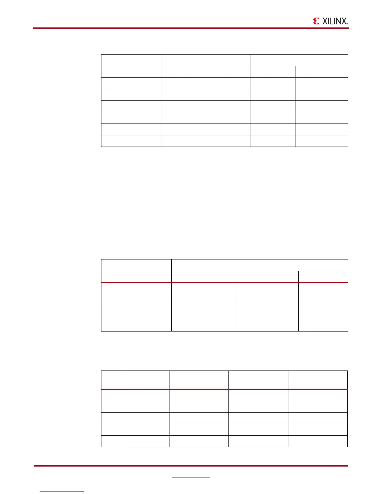
Table 1-10: SFP Module Connections
U1 FPGA Pin Schematic Net Name
P4 SFP Module Connector
Pin Number Pin Name
E3 SFP_RX_P 13 RDP_13
E4 SFP_RX_N 12 RDN_12
C3 SFP_TX_P 18 TDP_18
C4 SFP_TX_N 19 TDN_19
V23 SFP_LOS 8 LOS
AP12 SFP_TX_DISABLE
(1)
3TX_DISABLE
Notes:
1. The SFP TX Disable pin 3 is driven by transistor Q22, the base of which is driven
by the FPGA signal SFP_TX_DISABLE_FPGA.
Table 1-11: PHY Default Interface Mode
Mode
Jumper Settings
J66 J67 J68
GMII/MII to copper
(default)
Jumper over pins 1-2 Jumper over pins 1-2 No jumper
SGMII to copper,
no clock
Jumper over pins 2-3 Jumper over pins 2-3 No jumper
RGMII Jumper over pins 1-2 No jumper Jumper on
Table 1-12: Board Connections for PHY Configuration Pins
Pin
Connection on
Board
Bit[2]
Definition and Value
Bit[1]
Definition and Value
Bit[0]
Definition and Value
CFG0 V
CC
2.5V PHYADR[2] = 1 PHYADR[1] = 1 PHYADR[0] = 1
CFG1 Ground ENA_PAUSE = 0 PHYADR[4] = 0 PHYADR[3] = 0
CFG2 V
CC
2.5V ANEG[3] = 1 ANEG[2] = 1 ANEG[1] = 1
CFG3 V
CC
2.5V ANEG[0] = 1 ENA_XC = 1 DIS_125 = 1
CFG4 V
CC
2.5V HWCFG_MD[2] = 1 HWCFG_MD[1] = 1 HWCFG_MD[0] = 1

 Loading...


