14 www.xilinx.com ML605 Hardware User Guide
UG534 (v1.2.1) January 21, 2010
Chapter 1: ML605 Evaluation Board
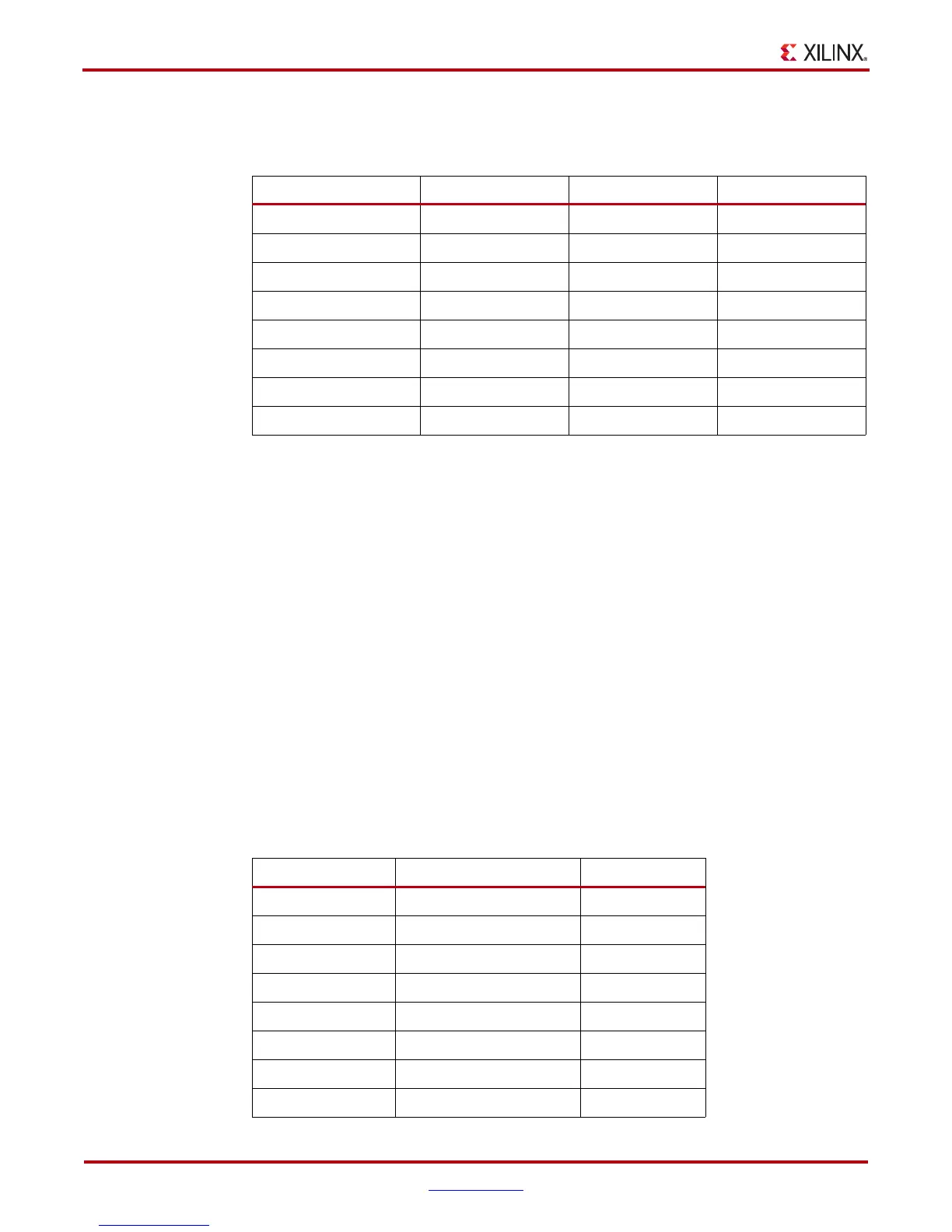
The ML605 supports Master BPI-Up, JTAG, and Slave SelectMAP. These are selected by
setting M[2:0] options 010, 101 and 110 shown in Table 1-2.
For an overview on configuring the FPGA, see “Configuration Options,” page 73.
Note:
The mode switches are part of DIP switch S2. The default mode setting (see Ta bl e A -1 ,
page 75) is M[2:0]=010, which selects Master BPI-Up at board power-on. Switch S1 position 4 must
be OFF to disable the System ACE controller from attempting to boot if a CF card is present.
References
See the Virtex-6 FPGA Configuration User Guide for detailed configuration information.
[Ref 5]
I/O Voltage Rails
There are 16 I/O banks available on the Virtex-6 device. The voltage applied to the FPGA
I/O banks used by the ML605 board is summarized in Table 1-3.
Table 1-2: Virtex-6 FPGA Configuration Modes
Configuration Mode M[2:0] Bus Width
(1)
CCLK Direction
Master Serial
(2)
000 1Output
Master SPI
(2)
001 1Output
Master BPI-Up
(2)
010 8, 16 Output
Master BPI-Down
(2)
011 8, 16 Output
Master SelectMAP
(2)
100 8, 16 Output
JTAG 101 1 Input (TCK)
Slave SelectMAP 110 8, 16, 32 Input
Slave Serial
(3)
111 1 Input
Notes:
1. The parallel configuration modes bus is auto-detected by the configuration logic.
2. In Master configuration mode, the CCLK pin is the clock source for the Virtex-6 FPGA internal
configuration logic. The Virtex-6 FPGA CCLK output pin must be free from reflections to avoid
double-clocking the internal configuration logic. See the Virtex-6 FPGA Configuration User Guide for
more details. [Ref 5]
3. This is the default setting due to internal pull-up termination on mode pins.
Table 1-3: Voltage Rails
U1 FPGA Bank I/O Rail Voltage
Bank 0 VCC2V5_FPGA 2.5V
Bank 12
(1)
FMC_VIO_B_M2C 2.5V
Bank 13 VCC2V5_FPGA 2.5V
Bank 14 VCC2V5_FPGA 2.5V
Bank 15 VCC2V5_FPGA 2.5V
Bank 16 VCC2V5_FPGA 2.5V
Bank 22 VCC2V5_FPGA 2.5V
Bank 23 VCC2V5_FPGA 2.5V

 Loading...


