EasyManua.ls Logo

Zynq UltraScale+ User Manual

Zynq UltraScale+
70 pages
To Next Page IconTo Next Page
To Previous Page IconTo Previous Page
Page #34 background imageLoading...
Page #34 background image
RFSoC Data Converter Evaluation Tool User Guide 34
UG1287 (v2018.2) October 1, 2018 www.xilinx.com
Chapter 4: Clocking
Resets
The following reset sources are in the design:
pl_resetn0 (from PS to PL)
This active Low reset is asserted by the PS during initialization.
ddr4_sync_rst (or c0_ddr4_ui_clk_sync_rst from the PL DDR memory interface group
(MIG))
This active High reset is asserted by the PL DDR MIG. It is synchronized to the UI clock
coming out the PL DDR MIG.
User-controlled reset block
This reset block is used to control the reset of FIFOs in both the RF-ADC datapaths
(adc_0, adc_1) and RF-DAC datapath (dac_0). It has an AXI4-Lite interface through which
the reset register can be accessed. Each bit of the register can be used to drive reset to
the block appropriately.
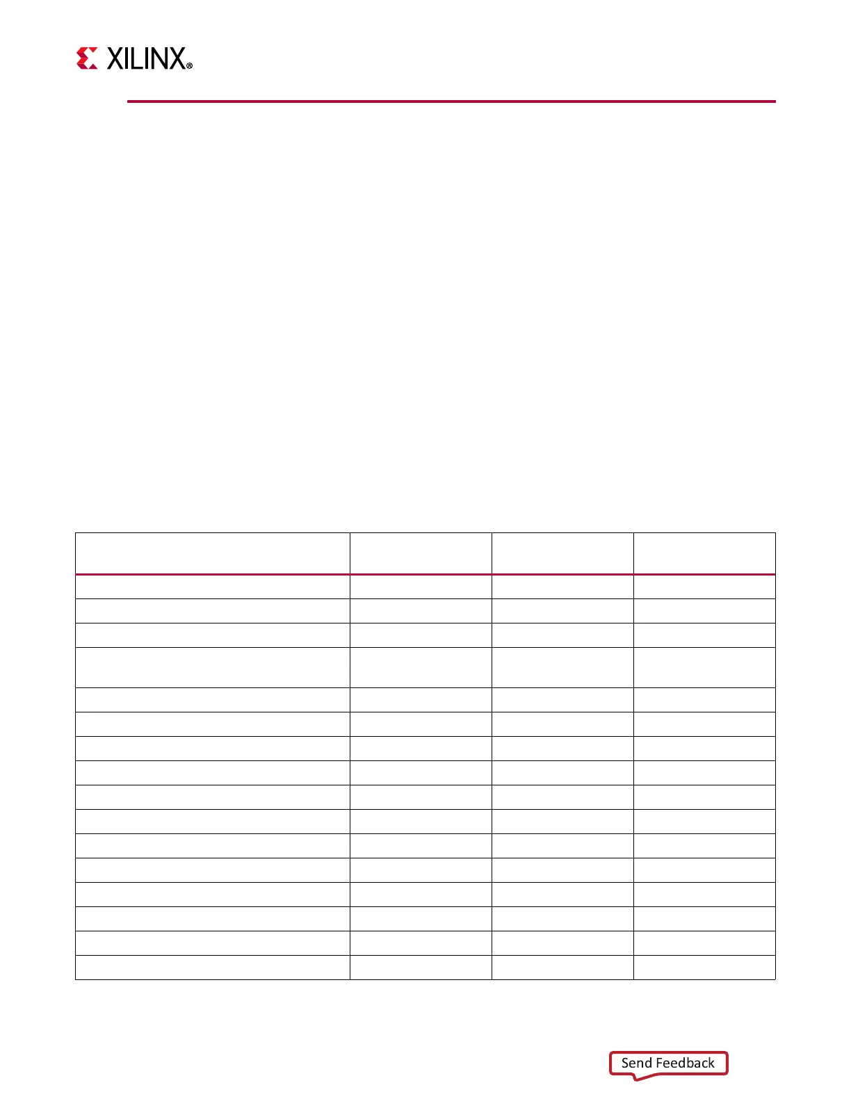
Table 4-3: Reset Distribution in the Evaluation Tool Design
Logic Block pl_resetn0 ddr4_sync_rst
User-controlled
Reset Block
PL DDR MIG X
DAC DMA X
ADC DMA X
RF data converter AXIS slave and master
interfaces (so, s1, and m0)
X
ADC_0 block AXIS data FIFO x (reset_0_n)
ADC_1 block AXIS data FIFO x (reset_1_n)
ADC_2 block AXIS data FIFO x (reset_2_n)
ADC_3 block AXIS data FIFO x (reset_3_n)
ADC_4 block AXIS data FIFO x (reset_4_n)
ADC_5 block AXIS data FIFO x (reset_5_n)
ADC_6 block AXIS data FIFO x (reset_6_n)
ADC_7 block AXIS data FIFO x (reset_7_n)
DAC 0 block- output AXIS data FIFOs x (dac reset_0_n)
DAC 1 block- output AXIS data FIFOs x (dac reset_1_n)
DAC 2 block- output AXIS data FIFOs x (dac reset_2_n)
DAC 3 block- output AXIS data FIFOs x (dac reset_3_n)
Send Feedback
Question and Answer IconNeed help?

Do you have a question about the Zynq UltraScale+ and is the answer not in the manual?

Zynq UltraScale+ Specifications

General IconGeneral
Max TransceiversUp to 32
Transceiver SpeedUp to 32.75 Gbps
FamilyZynq UltraScale+
Processor CoresQuad-core ARM Cortex-A53, Dual-core ARM Cortex-R5
Max MemoryDDR4
Power ConsumptionVaries by configuration, typically 10W to 30W
Operating TemperatureIndustrial (-40°C to +100°C), Extended (-40°C to +125°C)
Package OptionsVarious BGA packages
CategoryFPGA SoC

Summary

Chapter 1: Introduction to RF Data Converter Evaluation Tool

Zynq UltraScale+ RFSoC Overview

Describes the Zynq UltraScale+ RFSoC family, its integrated subsystems, and key capabilities for radio applications.

Reference Design Overview

Details the system-level block diagram, architecture, and components of the RF Data Converter evaluation tool.

Chapter 3: Hardware Design and Datapaths

Hardware Overview

Explains the Vivado IP integrator flow, hardware partitioning, and the overall hardware block diagram.

DAC Data Flow

Details the datapath implementation for the 8-channel RF-DAC, including sample storage and replay methods.

ADC Data Flow

Details the datapath implementation for the 8-channel RF-ADC, including IQ merge and channel selection.

Chapter 4: Clocking Architecture and Synchronization

Clocking Overview

Describes the clock domains, analog/mixed signal clocking structure, and PLLs used in the ZCU111 board.

Clock Switching Modes

Details support for multi-tile synchronization (MTS) and non-MTS modes, controlled by clock MUX.

Reset Sources and Distribution

Describes the different reset sources (PS, MIG) and their distribution to logic blocks and FIFOs.

Chapter 5: GUI-Based System Configuration

External Component Configuration

Explains GUI configuration of external PLLs, including frequency settings and DAC power modes.

ADC Configuration Details

Details GUI support for configuring ADC tiles, including ADCs, DDCs, clock generators, and PLLs.

ADC Clock Configuration

Describes GUI support for selecting and configuring external or internal sample clock options for ADCs.

DAC Configuration Options

Details GUI support for DAC configurations, including output current, linearity, and Nyquist zone operation.

DAC Clock Configurations

Describes GUI support for selecting and configuring external or internal sample clock options for DACs.

Chapter 6: Software Architecture

Software Platform Overview

Describes the software platform on the APU, the rftool application, and its interface to the GUI.

Chapter 7: Protocol Specification for Communication

Command Table Overview

Explains the string-based, space-separated command and response protocol for GUI-Linux application communication.

Multi-Tile Sync (MTS) Feature

Discusses the multi-tile synchronization feature for coordinated operation of multiple tiles.

Chapter 8: Bare-metal and Linux Driver Information

Linux Driver APIs

Refers to the description of Linux APIs for the Zynq UltraScale+ RFSoC Data Converter.

Chapter 9: System Considerations

Boot Process Sequence

Describes the non-secure boot flow and SD boot mode sequence, detailing component loading and execution.

Appendix A: Reference Design Protocol Specification