2-34 Block Diagrams
Block Diagrams The following pages contain the block diagrams for the PowerFlex 700
Vector Control drive.
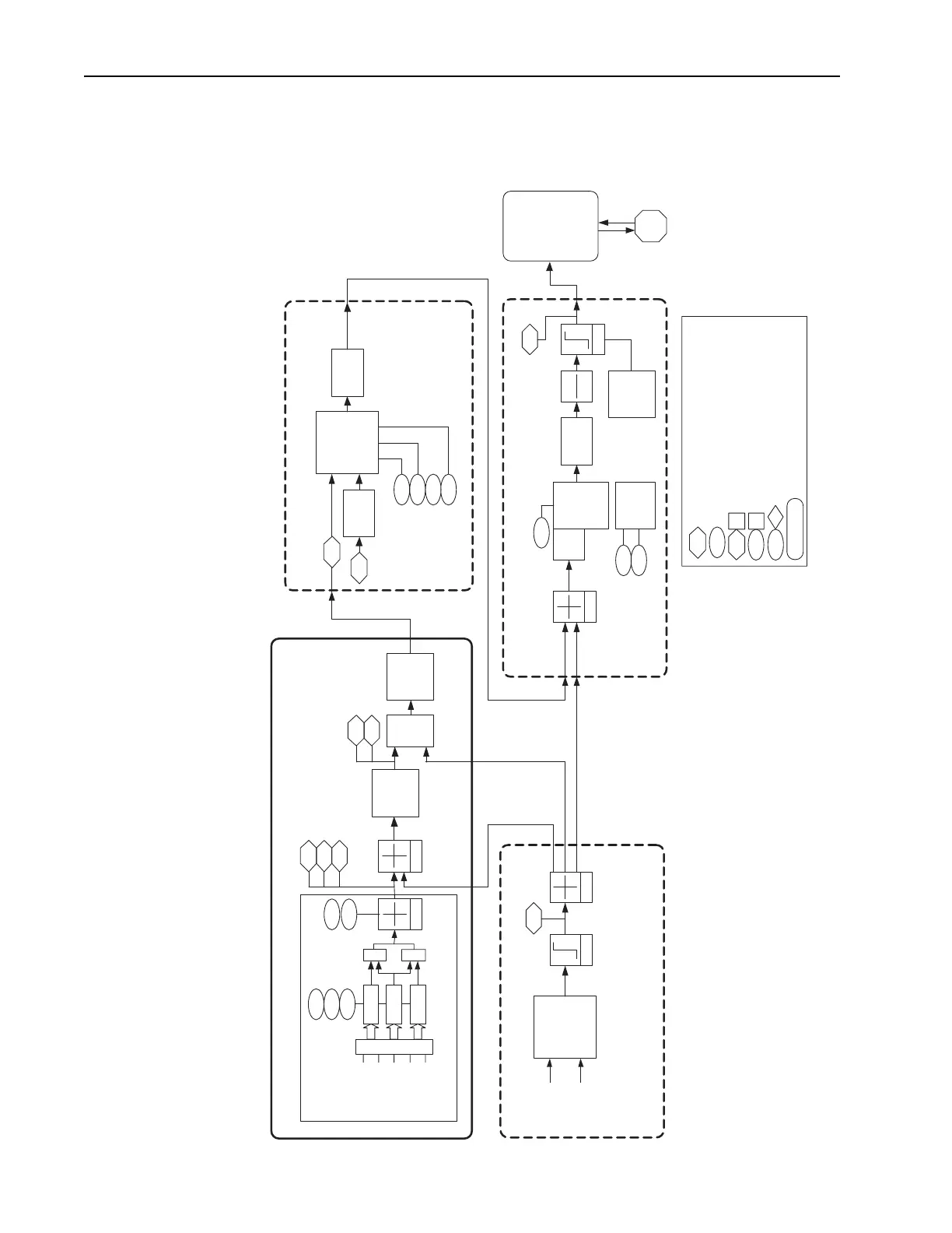
Figure 2.1 PowerFlex 700VC Block Diagams (1)
PowerFlex 700VC
Block Diagrams
Read Only Parameter
Read / Write Parameter
Read Only Parameter with Bit Enumeration
Read / Write Parameter with Bit Enumeration
Provides additional information
Read Testpoint with Data Select Value
PI Speed
Tr im
PI Excl
Mode
PI Regulator
446
445
Kp Speed Loop
Ki Speed Loop
Lead Lag
Lead Lag
25
Speed Control - Regulator (1.0ms)
Speed Reference
449
Speed Desired BW
23
447
Kf Speed Loop
Torque
Selection
*, /, +
Torque Trim
Bus Volt
& Power
Regulator
Notch
Control
Drive
& Motor
Protection
1
Flux
441
Mtr Tor Cur Ref
Torque Control (0.25ms)
Limit
88
Speed/Torque Mod
Logic
1 0
0 1
161
162
Bus Reg Mode A
Bus Reg Mode B
Spd Reg In
Vector
Control
Current
Processing
Motor
Vector Control Mode with Speed Control
Linear
Ramp &
S Curve
Min/Max
Limits
Commanded Speed
2
Speed Ref Selection
Speed Ref A Sel
117
90
93
+
Analog 1/2
Enc/Pulse
MOP
Presets 1-7
DPI Port 1-6
Spd Ref A
Spd Ref B
Tr i m
S
O
U
R
C
E
S
+
Speed Ref B Sel
Trim In Select
272
2
Commanded Freq
Drive Ref Rslt
22
273
Ramped Speed
Drive Ramp Rslt
+
Logic
1 0
0 1
Speed Control - Reference (2.0ms)
Logic
1 0
0 1
100
108
Jog Speed 1
Jog Speed 2
PI Regulator
PI Reference
PI Feedback
Limit
Process Control (2ms)
138
PI Output Meter
Logic
1 0
0 1
Speed
Feedback
(From Encoder)
 Loading...