118
IS42S16400F-6TL (HDMI : U1303, U2302)
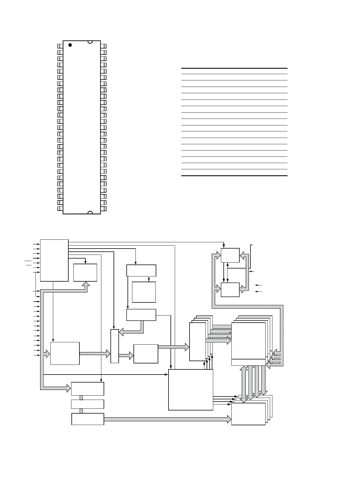
IS42S16400F-6TL Block Diagram
4 Integrated Silicon Solution, Inc. — www.issi.com
Rev. F
11/09/09
IS42S16400F
IS45S16400F
PIN CONFIGURATIONS
54 pin TSOP - Type II
PIN DESCRIPTIONS
A0-A11 RowAddressInput
A0-A7 Column Address Input
BA0,BA1 BankSelectAddress
DQ0toDQ15 DataI/O
CLK SystemClockInput
CKE ClockEnable
CS Chip Select
RAS RowAddressStrobeCommand
CAS Column Address Strobe Command
V
DD
DQ0
V
DD
Q
DQ1
DQ2
GNDQ
DQ3
DQ4
V
DD
Q
DQ5
DQ6
GNDQ
DQ7
V
DD
LDQM
WE
CAS
RAS
CS
BA0
BA1
A10
A0
A1
A2
A3
V
DD
1
2
3
4
5
6
7
8
9
10
11
12
13
14
15
16
17
18
19
20
21
22
23
24
25
26
27
54
53
52
51
50
49
48
47
46
45
44
43
42
41
40
39
38
37
36
35
34
33
32
31
30
29
28
GND
DQ15
GNDQ
DQ14
DQ13
V
DD
Q
DQ12
DQ11
GNDQ
DQ10
DQ9
V
DD
Q
DQ8
GND
NC
UDQM
CLK
CKE
NC
A11
A9
A8
A7
A6
A5
A4
GND
WE WriteEnable
LDQM x16LowerByte,Input/OutputMask
UDQM x16UpperByte,Input/OutputMask
Vdd Power
GND Ground
Vddq PowerSupplyforI/OPin
GNDq GroundforI/OPin
NC NoConnection
2 Integrated Silicon Solution, Inc. — www.issi.com
Rev. F
11/09/09
IS42S16400F
IS45S16400F
GENERAL DESCRIPTION
The 64Mb SDRAM is a high speed CMOS, dynamic
random-access memory designed to operate in 3.3V
memory systems containing 67,108,864 bits. Internally
congured as a quad-bank DRAM with a synchronous
interface. Each 16,777,216-bit bank is organized as 4,096
rows by 256 columns by 16 bits.
The64MbSDRAMincludesanAUTOREFRESHMODE,
and a power-saving, power-down mode. All signals are
registeredonthepositiveedgeoftheclocksignal,CLK.
AllinputsandoutputsareLVTTLcompatible.
The64MbSDRAMhastheabilitytosynchronouslyburst
data at a high data rate with automatic column-address
generation, the ability to interleave between internal banks
to hide precharge time and the capability to randomly
change column addresses on each clock cycle during
burst access.
A self-timed row precharge initiated at the end of the burst
sequenceisavailablewiththeAUTOPRECHARGEfunction
enabled.
Precharge
one bank while accessing one of the
other three banks will hide the
precharge
cycles and provide
seamless, high-speed, random-access operation.
SDRAM
read and write accesses are burst oriented starting
at a selected location and continuing for a programmed
number of locations in a programmed sequence. The
registration of an ACTIVE command begins accesses,
followedbyaREADorWRITEcommand.TheACTIVE
command in conjunction with address bits registered are
usedtoselectthebankandrowtobeaccessed(BA0,
BA1selectthebank;A0-A11selecttherow).TheREAD
or WRITE commands in conjunction with address bits
registered are used to select the starting column location
for the burst access.
ProgrammableREADorWRITEburstlengthsconsistof
1, 2, 4 and 8 locations, or full page, with a burst terminate
option.
CLK
CKE
CS
RAS
CAS
WE
A10
A9
A8
A7
A6
A5
A4
A3
A2
A1
A0
BA0
BA1
A11
COMMAND
DECODER
&
CLOCK
GENERATOR
MODE
REGISTER
REFRESH
CONTROLLER
REFRESH
COUNTER
SELF
REFRESH
CONTROLLER
ROW
ADDRESS
LATCH
MULTIPLEXER
COLUMN
ADDRESS LATCH
BURST COUNTER
COLUMN
ADDRESS BUFFER
COLUMN DECODER
DATA IN
BUFFER
DATA OUT
BUFFER
DQM
DQ 0-15
V
DD/VDDQ
GND/GNDQ
12
12
8
12
12
8
16
16 16
16
256K
(x 16)
4096
4096
4096
ROW DECODER
4096
MEMORY CELL
ARRAY
BANK 0
SENSE AMP I/O GATE
BANK CONTROL LOGIC
ROW
ADDRESS
BUFFER
4 Integrated Silicon Solution, Inc. — www.issi.com
Rev. F
11/09/09
IS42S16400F
IS45S16400F
PIN CONFIGURATIONS
54 pin TSOP - Type II
PIN DESCRIPTIONS
A0-A11 RowAddressInput
A0-A7 Column Address Input
BA0,BA1 BankSelectAddress
DQ0toDQ15 DataI/O
CLK SystemClockInput
CKE ClockEnable
CS Chip Select
RAS RowAddressStrobeCommand
CAS Column Address Strobe Command
V
DD
DQ0
V
DD
Q
DQ1
DQ2
GNDQ
DQ3
DQ4
V
DD
Q
DQ5
DQ6
GNDQ
DQ7
V
DD
LDQM
WE
CAS
RAS
CS
BA0
BA1
A10
A0
A1
A2
A3
V
DD
1
2
3
4
5
6
7
8
9
10
11
12
13
14
15
16
17
18
19
20
21
22
23
24
25
26
27
54
53
52
51
50
49
48
47
46
45
44
43
42
41
40
39
38
37
36
35
34
33
32
31
30
29
28
GND
DQ15
GNDQ
DQ14
DQ13
V
DD
Q
DQ12
DQ11
GNDQ
DQ10
DQ9
V
DD
Q
DQ8
GND
NC
UDQM
CLK
CKE
NC
A11
A9
A8
A7
A6
A5
A4
GND
WE WriteEnable
LDQM x16LowerByte,Input/OutputMask
UDQM x16UpperByte,Input/OutputMask
Vdd Power
GND Ground
Vddq PowerSupplyforI/OPin
GNDq GroundforI/OPin
NC NoConnection
4 Integrated Silicon Solution, Inc. — www.issi.com
Rev. F
11/09/09
IS42S16400F
IS45S16400F
PIN CONFIGURATIONS
54 pin TSOP - Type II
PIN DESCRIPTIONS
A0-A11 RowAddressInput
A0-A7 Column Address Input
BA0,BA1 BankSelectAddress
DQ0toDQ15 DataI/O
CLK SystemClockInput
CKE ClockEnable
CS Chip Select
RAS RowAddressStrobeCommand
CAS Column Address Strobe Command
V
DD
DQ0
V
DD
Q
DQ1
DQ2
GNDQ
DQ3
DQ4
V
DD
Q
DQ5
DQ6
GNDQ
DQ7
V
DD
LDQM
WE
CAS
RAS
CS
BA0
BA1
A10
A0
A1
A2
A3
V
DD
1
2
3
4
5
6
7
8
9
10
11
12
13
14
15
16
17
18
19
20
21
22
23
24
25
26
27
54
53
52
51
50
49
48
47
46
45
44
43
42
41
40
39
38
37
36
35
34
33
32
31
30
29
28
GND
DQ15
GNDQ
DQ14
DQ13
V
DD
Q
DQ12
DQ11
GNDQ
DQ10
DQ9
V
DD
Q
DQ8
GND
NC
UDQM
CLK
CKE
NC
A11
A9
A8
A7
A6
A5
A4
GND
WE WriteEnable
LDQM x16LowerByte,Input/OutputMask
UDQM x16UpperByte,Input/OutputMask
V
dd
Power
GND Ground
V
ddq
PowerSupplyforI/OPin
GND
q
GroundforI/OPin
NC NoConnection
 Loading...