27
AVR-2307CI / AVR-2307 / AVR-887 / AVC-1930
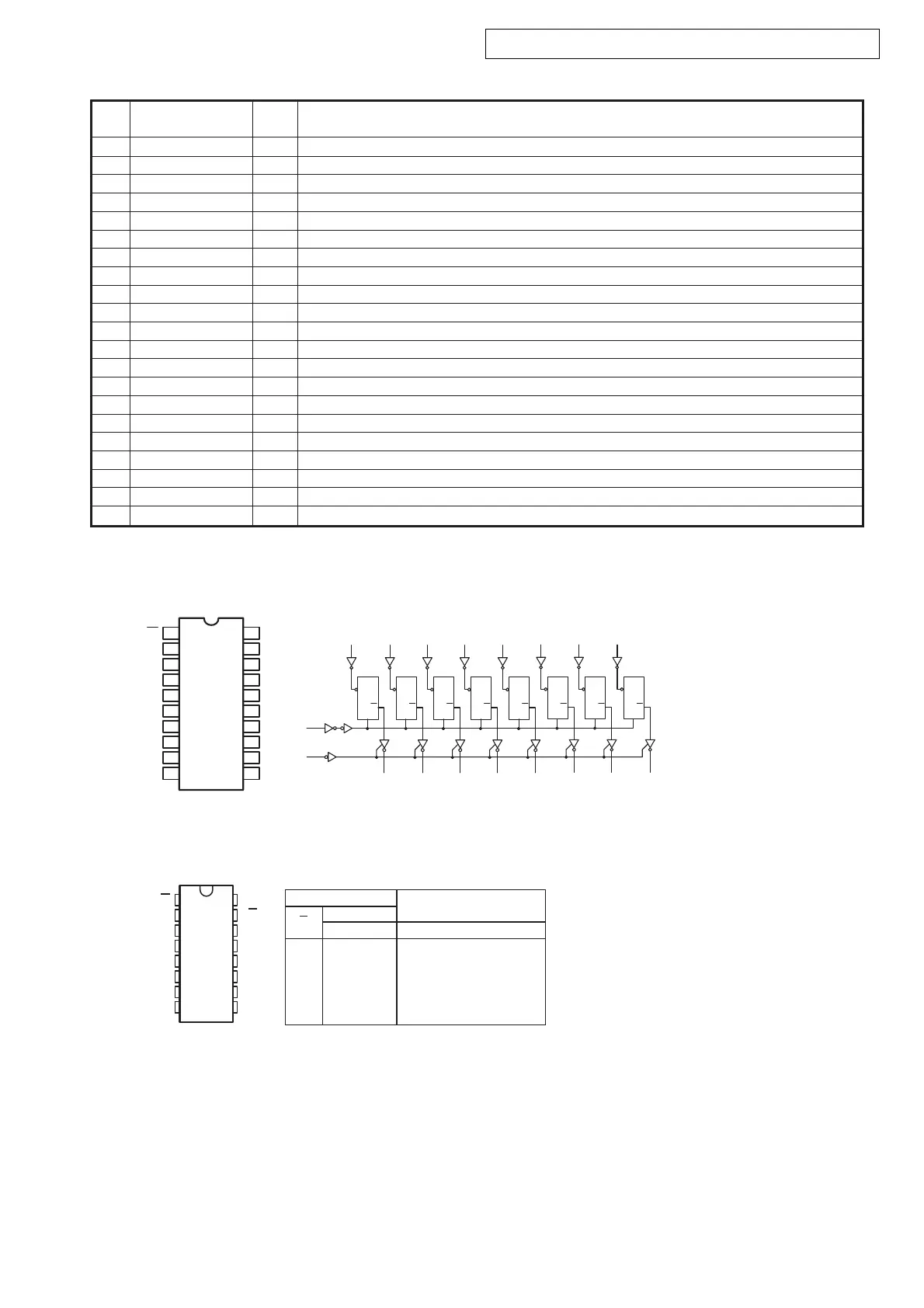
SN74LV573APWR (HDMI : IC818,819)
SN74LVC139APWR (HDMI : IC820)
Function
Pin
No.
Pin Name I/O
* For latch-up countermeasure, perform each power supply ON/OFF in the same timing.
28 XOUT O X’tal osc. connecting output terminal
29 XIN I X’tal osc. connection, external clock input terminal (24.576MHz or 12.288MHz)
30 DVDD — Digital power
31 DGND — Digital GND
32 EMPHA/UO I/O Emphasis information/U-data output/Chip address setting terminal
33 AUDIO/VO I/O Non-PCM detect/V-flag output/ Chip address setting terminal
34 CKST I/O Clock switch transition period output/Demodulation master or slave function switching terminal
35 INT I/O Interrupt output for
μ
μ
μ
μ
μ
com (Interrupt factor selectable)/Modulation or general I/O switching terminal
36 RERR O PLL lock error, data error flag output
37 DO O com I/F, read out data output terminal (3-state)
38 DI I com I/F, write data input terminal
39 CE I com I/F, chip enable input terminal
40 CL I com I/F, clock input terminal
41 XMODE I System reset input terminal
42 DGND — Digital GND
43 DVDD — Digital power
44 TMCK/PIO0 I/O 256fs system clock input for modulation/General I/O in/output terminal
45 TBCK/PIO1 I/O 64fs bit clock input for modulation/General I/O in/output terminal
46 TLRCK/PIO2 I/O fs clock input for modulation/General I/O in/output terminal
47 TDATA/PIO3 I/O Serial audio data input for modulation/General I/O in/output terminal
48 TXO/PIOEN O/I Modulation data output/ General I/O enable input terminal
1
2
3
4
5
6
7
8
10
9
20
19
18
17
16
15
14
13
12
11
OE
D0
D1
D2
D3
D4
D5
D6
D7
GND
Vcc
Q0
Q1
Q2
Q3
Q4
Q5
Q6
Q7
LE
D
Q
L
D
Q
L
D
Q
L
D
Q
L
D
Q
L
D
Q
L
D
Q
L
D
Q
L
D0
D1 D2
D3 D4 D5 D6
D7
L
E
OE
1
234
567
89
11
12131415
16
17
1819
Q0 Q1
Q2
Q3
Q4 Q5 Q6 Q7
1
2
3
4
5
6
7
8
16
15
14
13
12
11
10
9
1G
1A
1B
1Y0
1Y1
1Y2
1Y3
GND
V
CC
2G
2A
2B
2Y0
2Y1
2Y2
2Y3
FUNCTION TABLE
(each decoder/demultiplexer)
INPUTS
OUTPUTS
G
SELECT
OUTPUTS
G
B A Y3 Y2 Y1 Y0
L L L H H H L
L L HHHLH
L H LHLHH
L H HLHHH
H X X H H H H
 Loading...