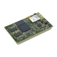
ConnectCore for i.MX51
©2011DigiInternational,Inc. 14
Module Pinout
The module has two 180-pin connectors, J1 and J2. The next tables describe each pin, its
properties, and its use on the module and development board. The DC parameters for each
I/O type are defined in the “I/O DC Parameters” section of Appendix A - Specifications.
The “Use on module” column shows the connection of the signals on the module. The format
of this column is “component: pad_name,” where “component” is the chip where the signals
are connected, and “pad_name” is the name of the pad where the signals are connected as
they are defined in the component’s datasheet.
Pinout Legend
I Input
OOutput
I/O Input or output
PPower
# Low level active signal
J1 Pinout
Pin I/O Type Signal name Use on module Use on development board Comments
1 GPIO27 CSI1_D8/GPIO3_12 i.MX51: CSI1_D8 Not used
2 GPIO27 CSI1_D9/GPIO3_13 i.MX51: CSI1_D9 Camera 1 Reset
3 HSGPIO27 CSI1_D10 i.MX51: CSI1_D10 Camera 1 data
4 HSGPIO27 CSI1_D11 i.MX51: CSI1_D11 Camera 1 data
5 HSGPIO27 CSI1_D12 i.MX51: CSI1_D12 Camera 1 data
6 HSGPIO27 CSI1_D13 i.MX51: CSI1_D13 Camera 1 data
7 HSGPIO27 CSI1_D14 i.MX51: CSI1_D14 Camera 1 data
8 HSGPIO27 CSI1_D15 i.MX51: CSI1_D15 Camera 1 data
9 HSGPIO27 CSI1_D16 i.MX51: CSI1_D16 Camera 1 data
10 HSGPIO27 CSI1_D17 i.MX51: CSI1_D17 Camera 1 data
11 HSGPIO27 CSI1_D18 i.MX51: CSI1_D18 Camera 1 data
12 HSGPIO27 CSI1_D19 i.MX51: CSI1_D19 Camera 1 data
13 GPIO27 CSI1_VSYNC/GPIO3_14 i.MX51: CSI1_VSYNC Camera 1 vertical synchronization
14 GPIO27 CSI1_HSYNC/GPIO3_15 i.MX51: CSI1_HSYNC Camera 1 horizontal
synchronization
15 GPIO27 CSI1_PIXCLK i.MX51: CSI1_PIXCLK Camera 1 pixel clock
16 GPIO27 CSI1_MCLK i.MX51: CSI1_MCLK Camera 1 & 2 Master clock
17 - GND - -
 Loading...