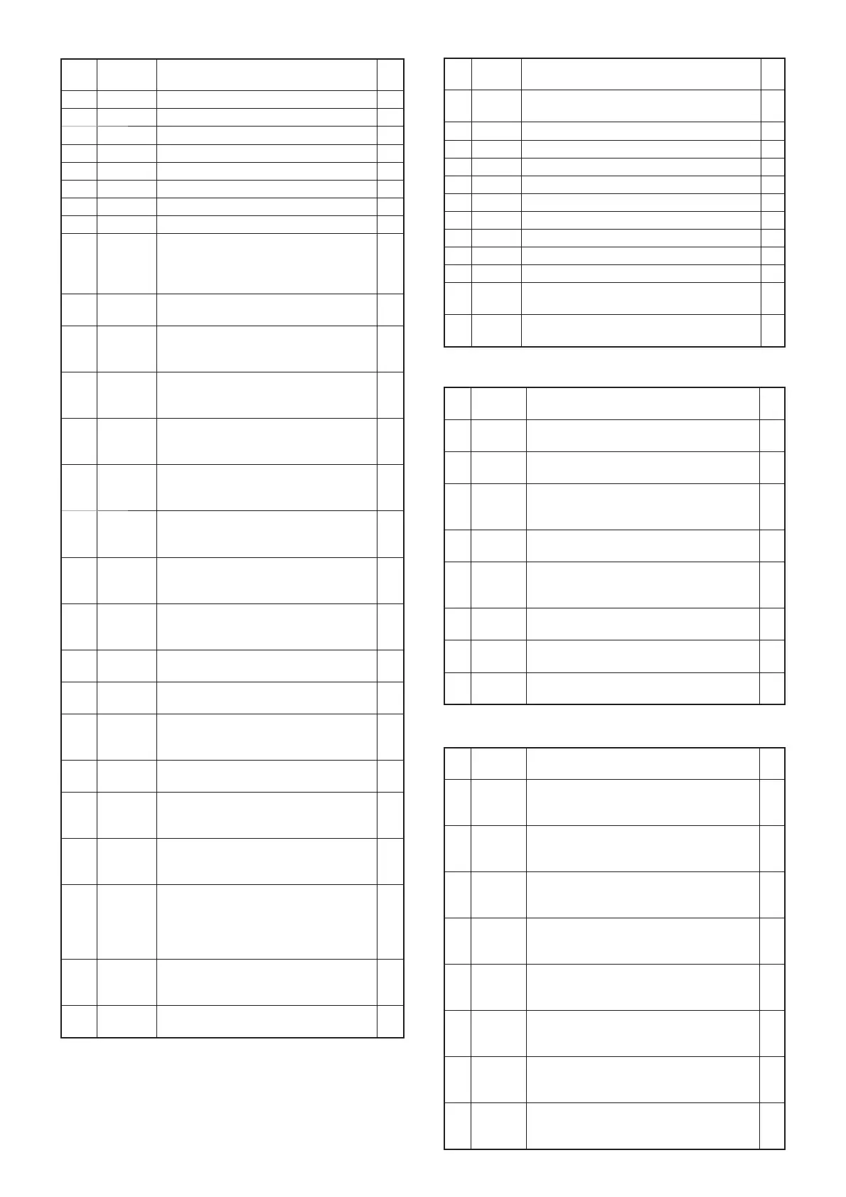
3-11
PIN
No.
LINE
NAME
DESCRIPTION I/O
1 ICCV APC AMP reference voltage. O
2 FANV Cooling fan rotation control voltage. O
15 3DST 3rd LO DDS strobe. O
16 1CN1 1st Lo DDS control bit. (OSK) O
17 1CN0 1st Lo DDS control bit. (IOUPDATE) O
18 1DST 1st Lo DDS strobe. O
19 PDAT DDS serial data. O
20 PCK DDS serial clock. O
21 HTXS The HF/50 MHz/70 MHz band TX circuit
control.
High= While transmitting on the HF/50
MHz/70 MHz band.
O
22 VTXS The VHF band TX circuit control.
High=While transmitting on the VHF band.
O
23 UTXS The UHF band TX circuit control.
High= While transmitting on the
HF/50 MHz/70 MHz band.
O
24 LOF5 1st LO fi lter select.
High= While operating on 148.000000 to
199.999999 MHz.
O
25 LOF6 1st LO fi lter select.
High= While operating on 400.000000 to
470.000000 MHz.
O
28 LOF4 1st LO fi lter select.
High= While operating on 115.5130000 to
148.000000 MHz.
O
29 LOF3 1st LO fi lter select.
High= While operating on 60.000000 to
115.512999 MHz.
O
30 LOF2 1st LO fi lter select.
High= While operating on 15.000000 to
59.999999 MHz.
O
31 LOF1 1st LO fi lter select.
High= While operating on 0.030000 to
14.999999 MHz.
O
33 TCON External antenna tuner connection detect.
Low=An antenna tuner is connected.
I
34 MMSL Microphone type detect.
Low=HM-151 is connected.
I
36 RSPK Speaker plug insertion detect.
High= A speaker is connected on the rear
speaker jack.
I
39 PRESL DDS reset.
Low=Reset.
O
40 DBRS 1st LO fi lter select.
High= While operating on 30.000000 to
470.000000MHz.
O
44 DLF1 DDS fi lter switching control.
High= While operating on 30.000000 to
107.999999 MHz.
O
47 DLF2 DDS fi lter switching control.
High=While operating on
0.030000 to 29.999999 MHz,
108.000000 to 199.999999 MHz or
400.000000 to 470.000000 MHz
O
51 DLF3 DDS fi lter switching control.
High= While operating on 0.030000 to
199.999999 MHz.
O
54 TXS TX circuit (All bands) control.
High=While transmitting.
O
• SUB CPU (MAIN UNIT: IC6401) • D/A CONVERTER (MAIN UNIT: IC7006)
• EXPANDER (MAIN UNIT: IC7001)
• EXPANDER (MAIN UNIT: IC7002)
PIN
No.
LINE
NAME
DESCRIPTION I/O
2 VUID1V VHF/UHF band TX power AMP iding current
control.
O
3 DIDV TX drive AMP iding current control. O
4 VUT1V VHF/UHF band BPF tuning voltage. (1 of 2) O
5 VUT2V VHF/UHF band BPF tuning voltage. (2 of 2) O
6 VTRV VHF band 1st IF trap circuit tuning voltage. O
7 BANV Operating band selecting voltage. O
8 POCV TX output power control voltage. O
9 DRIV TX drive AMP gain control voltage. O
12 IFT1V 1st IF fi lter tuning voltage. (1 of 2) O
13 IFT2V 1st IF fi lter tuning voltage. (2 of 2) O
18 HFID1V HF/50 MHz/70 MHz band TX power AMP idling
current control. (1 of 2)
O
19 HFID2V HF/50 MHz/70 MHz band TX power AMP idling
current control. (2 of 2)
O
PIN
No.
LINE
NAME
DESCRIPTION I/O
1 UPRES UHF band pre-AMP control.
Low=The Pre-AMP is ON.
O
2 VUATTS 144/430 MHz band attenuator control.
High=Attenuator ON.
O
3 VBANDS VHF band tuned BPFs switching.
High= While operating on the VHF band
(74.800000 to 128.999999 MHz).
O
4 FMS Operating mode select.
High=While operating in the FM or DV mode.
O
5 NASBS Operating mode select.
High= While operating in the mode other than
SSB or AM.
O
6 AMS AM mode select.
High=While operating in the AM mode
O
7 WFMS WFM mode select.
High=While operating in the WFM mode
O
15 VPRES VHF band pre-AMP control.
Low=The Pre-AMP is ON.
O
PIN
No.
LINE
NAME
DESCRIPTION I/O
1 B1 HF/50 HMz/70 MHz band select.
High= While operating on 1.600000 to
1.999999 MHz
O
2 B2 HF/50 HMz/70 MHz band select.
High= While operating on 2.000000 to
3.399999 MHz
O
3 B3 HF/50 HMz/70 MHz band select.
High= While operating on 3.400000 to
6.899999 MHz
O
4 B4 HF/50 HMz/70 MHz band select.
High= While operating on 6.900000 to
13.899999 MHz
O
5 B5 HF/50 HMz/70 MHz band select.
High= While operating on 13.900000 to
20.899999 MHz
O
6 B6 HF/50 HMz/70 MHz band select.
High= While operating on 20.900000 to
39.999999 MHz
O
7 B7 HF/50 HMz/70 MHz band select.
High= While operating on 40.000000 to
59.999999 MHz
O
15 B0 HF/50 MHz/70 MHz band BPFs switching.
High= While operating on 0.030000 to
1.599999 MHz
O
 Loading...