SECTION 4
THEORY OF OPERATION
4.1 INTRODUCTION
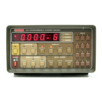
This section contains circuit descriptions of the Model 224.
The information is arranged to provide a circuit description of
individual functional circuit blocks. To facilitate understand-
ing the descriptions are keyed to accompany simplified block
diagrams and schematics. Detailed schematics of the Model
224 are located in Section 6.
4.2 BLOCK DIAGRAMS
The circuitry of the Model 224 is represented by the two
simplified block diagrams in Figures 4-l and 4-2. Figure 4-l
shows a simplified block diagram of the Model 224’s
analog
circuitry (power supply, range circuitry, amplifiers etc.).
Figure 4-2 shows a simplified block diagram of the Model
224’s digital circuitry (microprocessor, RAM, ROM, VIA
etc.).
4.3 POWER SUPPLY
To facilitate understanding of the following discussion refer
to schematic diagram 220-106 (sheet 2 of 2). The power sup-
ply is a conventional AC to DC power converter. Transformer
TlOl, has three separate secondaries that are fed into three
separate bridge rectifiers CRIOI, CR108 and the bridge con-
figuration of CR102 through CR105. The output of CR101 is
fed into the regulator VRlOl and is filtered by Cl07 and Cl03
producing the +5V digital supply. The output of CR108 is fed
into VR102 and VR103 and is filtered by Cl19 through Cl22
to produce the positive and negative 15V supplies. The out-
put of CR102 through CR105 is filtered by Cl 17 and Cl 18 to
produce the positive and negative 125V supplies. R118 and
RI19 are bleeder resistors to prevent charge retention after
the AC power is removed.
A tap off of the primary of the transformer TIOI, supplies the
nominal 115VAC to the ventilation fan.
4.4 ANALOG BOARD
To faciliate understanding of the following discussion refer to
schematic diagram number 224-126.
The heart of the analog board is the high voltage op amp
which is centered around U319. The performance of U319 is
bootstrapped up to the voltage levels supplying Q318 and
0319 by Q315Q319, Q313Q318 and their associated cir-
cuitry. 0310, 0302, R344, R348, R349, C313 and C320
establish frequency stability for U319. R343 is an input
voltage offset adjustment for U319.
A constant current source can be derived by a series voltage
source and resistance from the output (analog/common/
guard) to the amplifier input. The amplifier input to the com-
mon of the high voltage supplies of Q318/Q319 (output com-
mon) comprised a current source. Range resistors (R375,
R376, R377, R379, R380, R381 and R383) along with their
associated calibration potentiometers make up the series
resistance section of the current source. When more than
one resistance is connected through one relay, JFET-
switches are used to distinguish which resistor is being used.
Several JFETs are organized in pairs for voltage sensing at
the resistor to compensate for the voltage drop in the current
carrying JFET.
U315 serves as sense amplifier with Q311, 0312, R344 and
R345 as a high current buffer for the higher current ranges.
U314, U318A and U320B,C,D,E and F drive the range relays.
U313 and U317 are voltage comparators with open collector
outputs. Combined with R350, this circuitry provides the
voltage drive for the switching FETs.
The voltage source section centers around U311, the 12 bit
digital-to-analog converter (DACI. Associated circuitry R301
through R307 and R316, are used to adjust offset and
positive gain. Gain is set on the ImA range and therefore
does not require an adjustment. Following this circuitry is a
network providing a + operator to the output of U311. U312
provides the active portion, while switches on U306 align
with resistors R317, R318, R320 and R323 to provide a select-
able gain of + 1 or -1.
R318 provides a gain adjust (-1mA) for this operator. The out-
put is fed to the sense amplifier U315. R392 is an offset
voltage adjustment potentiometer for U312 and U315.
Serial to parallel shift/store registers U301, U302 and U303
provide digital control from the serial data link. Data is
transmitted via the clock and latch lines. Latch selects the
data in mode as either recirculated data out (latch = logic 0) or
the over compliance V-limit information (latch = logic 1).
This selection is performed by U304A and B, U316B and C,
and U305A.
Gates U305B, C and D form a flip-flop for controlling the
tristate mode of the outputs of U301, U302 and U303. This
circuitry, along with R351, R352, CR307, C305, etc.,
prevents erroneous current source outputs both on acquisi-
tion and loss of AC line power.
The remaining portion of the analog circuitry produces the
selectable compliance voltage limit. An 8 bit digital-to-analog
converter (DACI U308 starts this process. With 128 combina-
tions, each step is scaled to represent 1V of compliance.
Since U308 is a current output DAC, U309 is required to
4-l
 Loading...