Process data transfer
Lenze device control
Process data signals for 8200 vector frequency inverters
7
l
53
EDSMF2133IB EN 5.0
Device status word AIF−STAT for 8200 vector (C0150, index 5F69
hex
)
Bit Assignment (Lenze setting) Set under C0417/...
0 Current parameter set (DCTRL−PAR−B0) 1
1 Pulse inhibit (DCTRL1−IMP) 2
2 I
max
limit (MCTRL1−IMAX) 3
3 Output frequency = frequency setpoint (MCTRL1−RFG1=NOUT) 4
4 Ramp function generator input = ramp function generator output 1
(NSET1−RFG1−I=0)
5
5 Q
min
threshold (PCTRL1−QMIN) 6
6 Output frequency = 0 (DCTRL1−NOUT=0) 7
7 Controller inhibit (DCTRL1−CINH) 8
8 ... 11 Device status (DCTRL1−Stat*1 ... STAT*8)
Reserved
Bit 11 10 9 8
0 0 0 0 Device initialisation
0
0 1 0 Switch−on inhibit
0
0 1 1 Operation inhibited
0
1 0 0 Flying restart circuit active
0 1 0 1 DC injection brake active
0
1 1 0 Operation enabled
0
1 1 1 Message active
1
0 0 0 Fault active
1
1 1 1 Communication with basic device not possible
12 Overtemperature warning (DCTRL1−OH−WARN) 13
13 DC−bus overvoltage (DCTRL1−OV) 14
14 Direction of rotation (DCTRL1−CCW) 15
15 Ready for operation (DCTRL1−RDY) 16
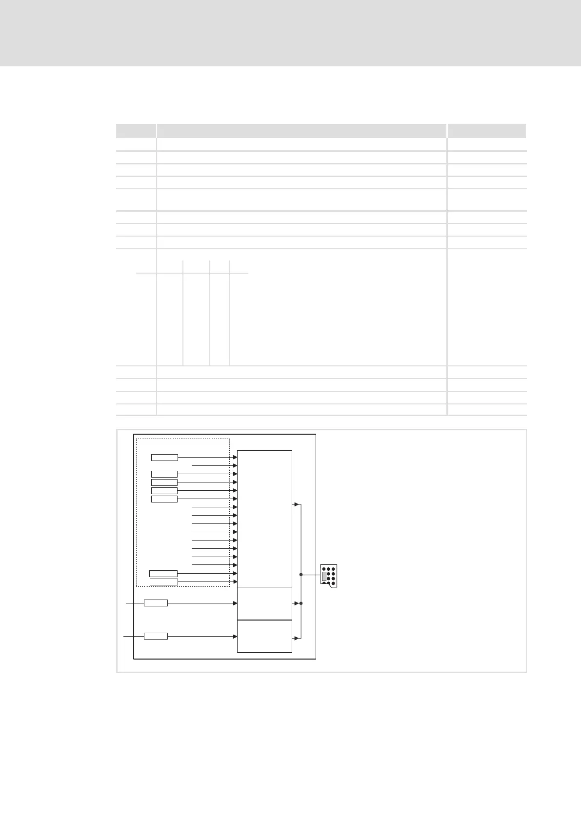
AIF-OUT
AIF-STAT
16 Bit
16 Bit
.B15
.B12
.B0
.B1
.B2
.B3
.B4
.B8
.B9
.B10
.B11
16 Bit
.B13
.B14
.B5
.B6
.B7
.B0
C0417/1
AIF-OUT.W1
AIF-OUT.W2
.B1
DCTRL1-IMP
.B2
C0417/3
.B3
C0417/4
.B4
C0417/5
.B5
C0417/6
.B6
DCTRL1-NOUT=0
.B7
DCTRL1-CINH
.B8
DCTRL1-STAT*1
.B9
DCTRL1-STAT*2
.B10
.B11
DCTRL1-STAT*4
DCTRL1-STAT*8
.B12
DCTRL1-OH-WARN
.B13
DCTRL1-OV
.B14
C0417/15
.B15
C0417/16
AIF
STAT1
C0421/1
C0421/2
2141LON013
Fig. 7−4 System block AIF−OUT in 8200 vector (freely programmable assignment)
 Loading...