6-8 VHF Theory of Operation: Frequency Generation Circuitry
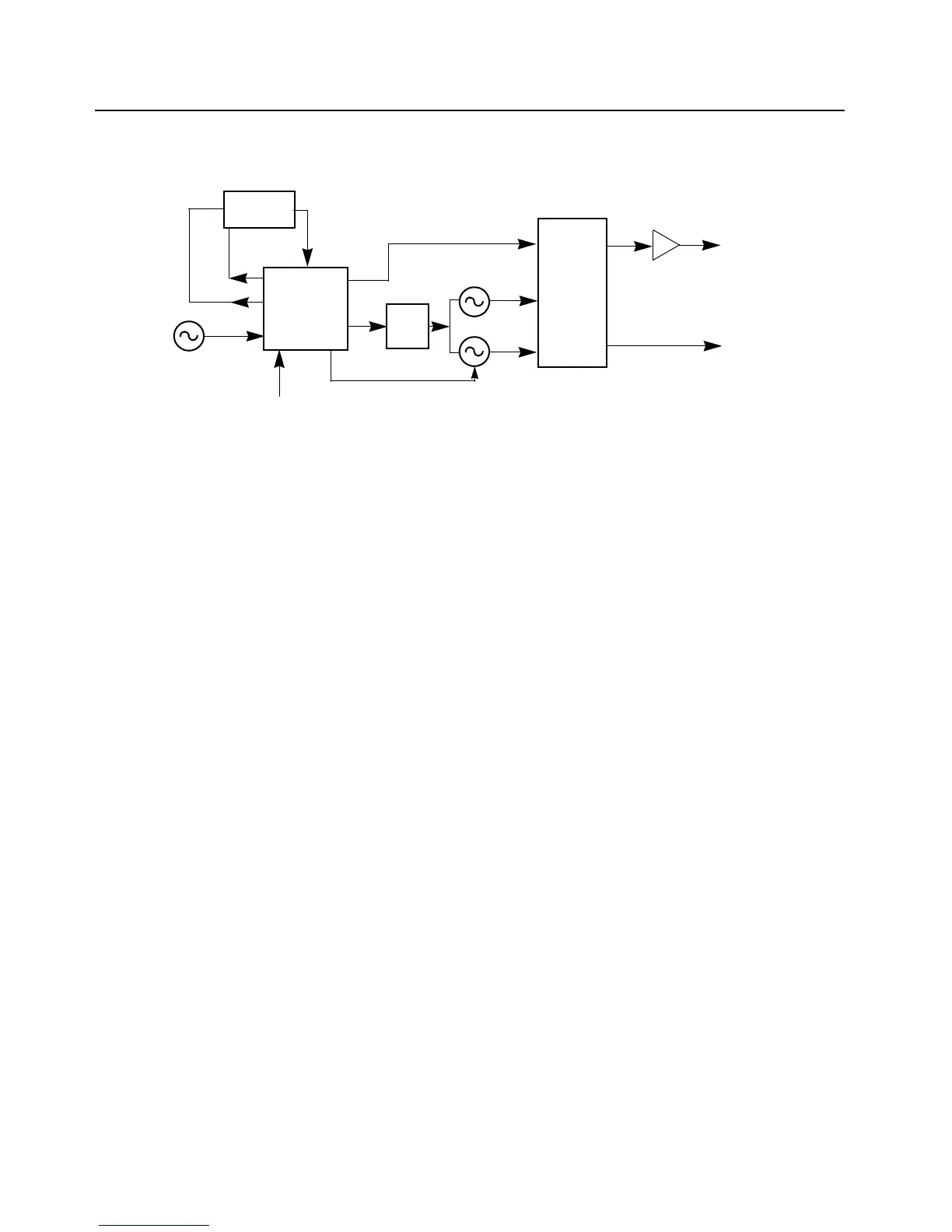
6.4 Frequency Generation Circuitry
Figure 6-4. Frequency Generation Unit Block Diagram
The Frequency Generation Circuitry is composed of two main ICs, the Fractional-N synthesizer
(U3701), and the VCO/Buffer IC (U3801). Designed in conjunction to maximize compatibility, the two
ICs provide many of the functions that normally would require additional circuitry. The synthesizer
block diagram illustrates the interconnect and support circuitry used in the region. Refer to the
relevant schematics for the reference designators.
The synthesizer is powered by regulated 5 V and 3.3 V which come from U3711 and U3201
respectively. The synthesizer in turn generates a superfiltered 4.5 V which powers U3801.
In addition to the VCO, the synthesizer must interface with the logic and ASFIC circuitry.
Programming for the synthesizer is accomplished through the data, clock and chip select lines from
the microprocessor. A 3.3 V dc signal from synthesizer lock detect line indicates to the
microprocessor that the synthesizer is locked.
Transmit modulation from the ASFIC is supplied to pin10 of U3701. Internally the audio is digitized
by the Fractional-N and applied to the loop divider to provide the low-port modulation. The audio runs
through an internal attenuator for modulation balancing purposes before going out to the VCO.
Voltage
Multiplier
Synthesizer
U3701
Loop
Filter
VCOBIC
U3801
To
Mixer
To
PA Driver
VCP
Vmult1
Aux3
MOD Out
Modulating
Signal
Vmult2
Rx VCO Circuit
Tx VCO
TRB
16.8 MHz
Ref. Osc.
Rx Out
Tx Out
Circuit
 Loading...