Low Band, 800 MHz, PassPort & 900 MHz Theory of Operation: Frequency Generation Circuitry 7-21
The IF automatic gain control circuit provides approximately 50 dB of attenuation range. The signal
strength indicator (RSSI) output of the IF IC produces a voltage that is proportional to the RF level at
the IF input to the IF IC. This voltage is inverted by U350, R351, R353, R352, R354 and C355 and it
determines the RF level at which the backend end AGC is activated as well as the slope of the
voltage at the output of U350 vs. the strength of the incoming RF at the antenna. The inverted output
of U350 is applied to the second gate of the IF amplifier U352 via R355. As the RF signal into the IF
IC increases the following occurs:
• The RSSI voltage increases,
• The output of inverter U350 decreases, and
• The voltage applied to the second gate of the FET is reduced thus reducing the gain of the IF
amplifier.
The output of inverter U350 is also used to control the receiver front end AGC.
The receiver front end automatic gain control circuit provides and additional 20 dB of gain reduction.
The output of the receiver back end inverter U350 is fed into the receiver front end AGC inverter
U302. The components R317, R314, and C318 determine:
• The RF level at which the front end AGC is activated, and
• The slope of the voltage at the output of U302 vs. the strength of the incoming RF at the antenna.
As the RF into the antenna increases the following occurs:
• The output voltage of the receiver back end inverter U350 decreases.
• The voltage at the output of the front end inverter U302 increases.
• The result is the forward biasing of pin diode CR301.
As the diode becomes more and more forward biased the following occurs:
• C310 loads the output of the low noise amplifier Q302 thus reducing the gain of the low noise
amplifier.
• R315 and R318 provide a DC path for CR301 and also limit the current through CR301.
The blocking capacitor C317 prevents DC from the AGC stage from appearing at the input of the
filter FL301.
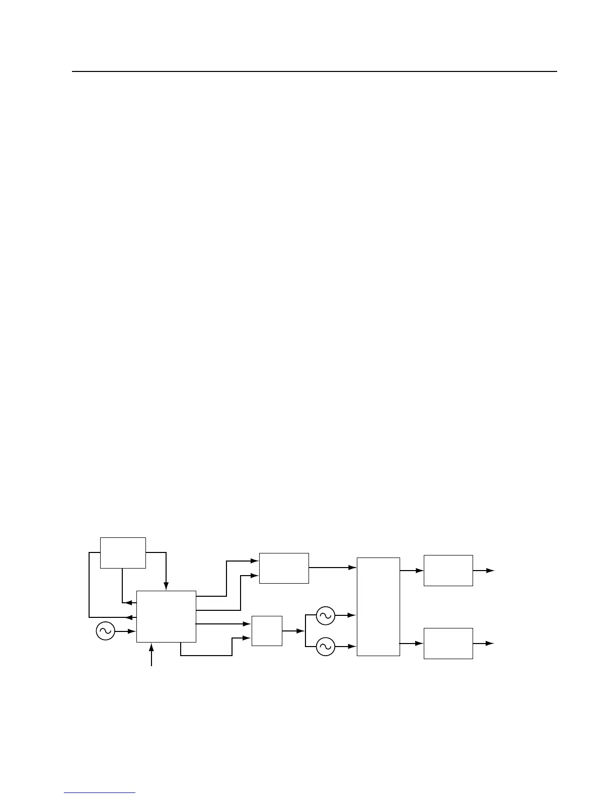
7.12 Frequency Generation Circuitry
Figure 7-12. Frequency Generation Unit Block Diagram
Synthesizer
U201
VCOBIC
U250
Voltage
Multiplier
Dual
Transistor
Loop
Filter
Injection
Amplifier
Buffer
Amplifier
To Mixer
To PA Driver
VCP
Vmult1
Vmult2
Aux3
Aux4
MOD Out
Modulating
Signal
Rx VCO
Circuit
Tx VCO
Circuit
TRB
16.8 MHz
Ref. Osc.
Rx
Out
Tx
Out
 Loading...