7-1
Chapter 7 Low Band, 800 MHz, PassPort & 900 MHz
Theory of Operation
7.1 Introduction
This chapter provides a detailed theory of operation for the radio components. Schematic diagrams
for the circuits described in the following paragraphs are located in Figures 9-238 through 9-284.
7.2 Low Band Transmitter
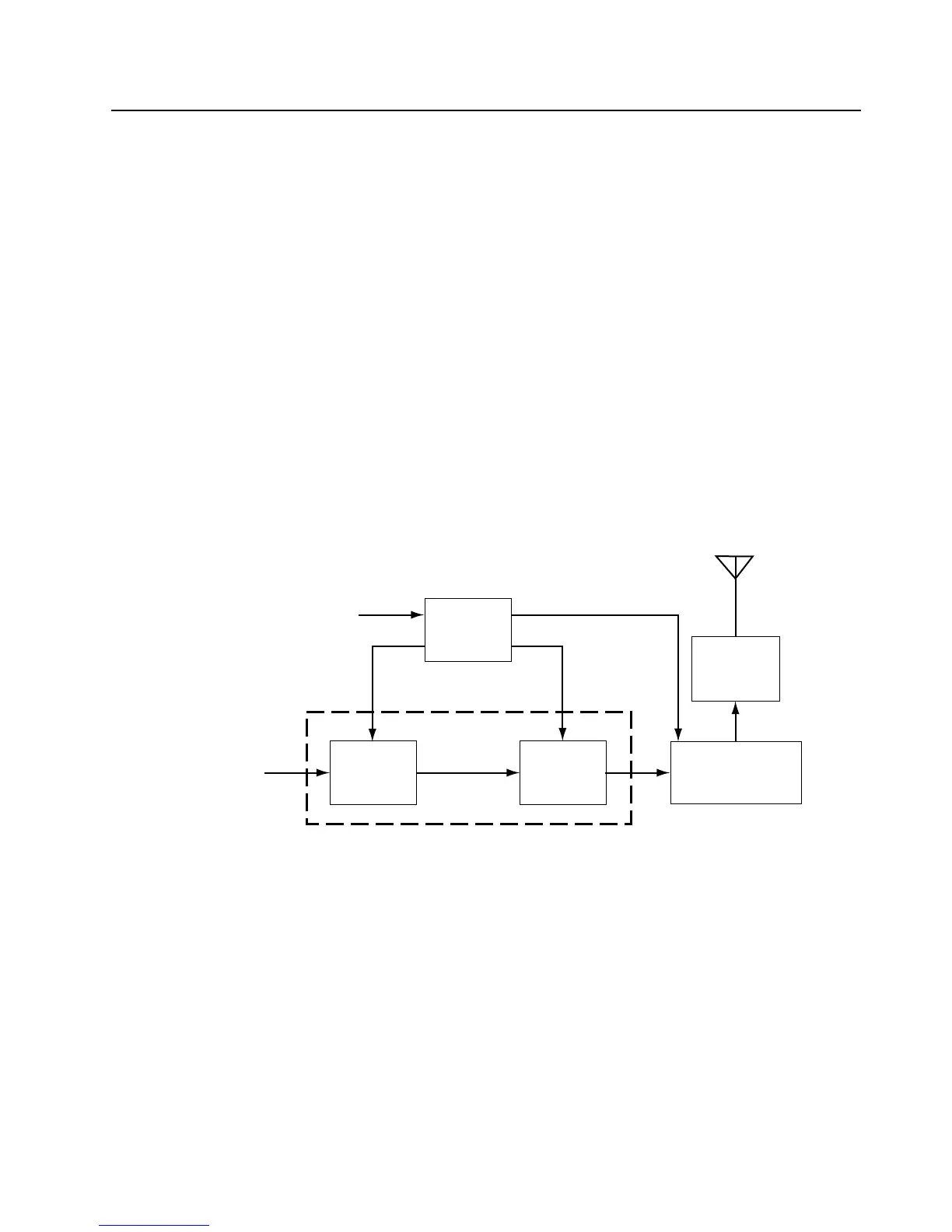
The low band transmitter consists of the following basic circuits as shown in Figure 7-1.
• Power amplifier (PA).
• Antenna switch/harmonic filter.
• Antenna matching network.
• Power control integrated circuit (PCIC).
Figure 7-1. Low Band Transmitter Block Diagram
7.2.1 Power Amplifier (PA)
The PA consists of two LDMOS devices:
• PA driver, U101.
• PA final stage, Q100.
The LDMOS driver (U101) provides 2-stage amplification using a supply voltage of 7.3V. The
amplifier is capable of supplying an output power of 0.3 W (pins 6 and 7) with an input signal of 2mW
at (pin16). The current drain is typically 120 mA while operating in the frequency range of 29.7 -
50 MHz. The power output of this stage is varied by the power control loop which controls the voltage
on pin 1.
PCIC
PA
Driver
Antenna Switch/
Harmonic Filter
PA Final
Stage
Vcontrol
SPI Bus
Gate Bias
Antenna Switch Bias
Antenna
Matching
Network
From VCO
Power Amplifier (PA)
 Loading...