Low Band, 800 MHz, PassPort & 900 MHz Theory of Operation: 800 MHz Receiver 7-11
• The RF level at which the front end AGC is activated, and
• The slope of the voltage at the output of U302 vs. the strength of the incoming RF at the antenna.
As the RF into the antenna increases the following occurs:
• The output voltage of the receiver backend inverter U350 decreases.
• The voltage at the output of the front end inverter U302 increases.
• The result is the forward biasing of pin diode CR301.
As the diode becomes more and more forward biased the following occurs:
• C310 loads the output of the low noise amplifier Q302 thus reducing the gain of the low noise
amplifier.
• R315 and R318 provide a DC path for CR301 and also limit the current through CR301.
The blocking capacitor C317 prevents DC from the AGC stage from appearing at the input of the
filter FL301.
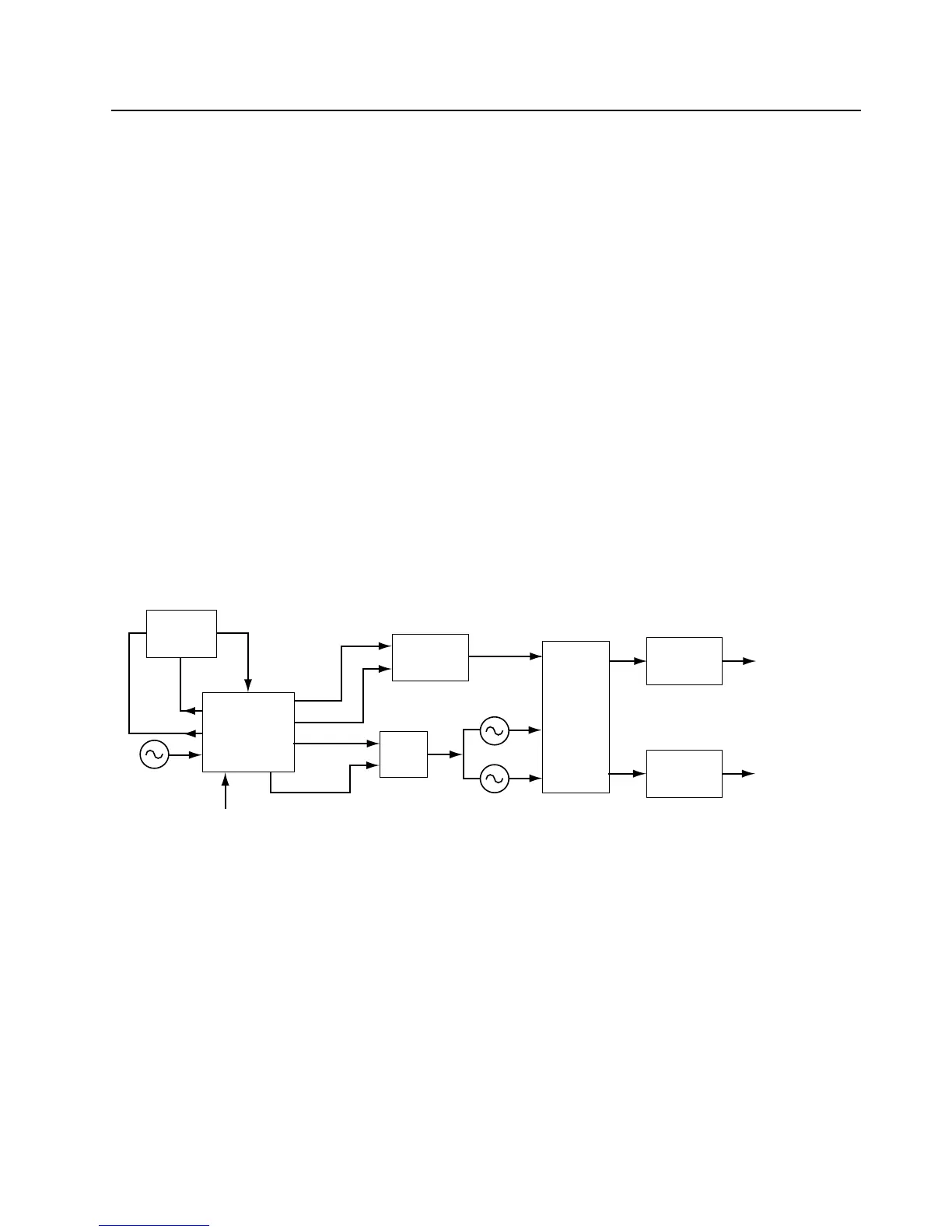
7.7.4 Frequency Generation Circuit
The frequency generation circuit is shown in Figure 7-7. The circuit is composed of the two main ICs:
• Low Voltage Fractional-N Synthesizer, U201
• VCO/Buffer IC, U250
Figure 7-7. 800 MHz Frequency Generation Unit Block Diagram
Designed in conjunction to maximize compatibility, the two ICs provide many of the functions that
normally would require additional circuitry. The synthesizer block diagram illustrates the interconnect
and support circuitry used in the region. Refer to the relevant schematics for the reference
designators.
The synthesizer is powered by regulated 5 V and 3.3 V which come from U247 and U248
respectively. The synthesizer in turn generates a superfiltered 4.5 V which powers U250.
In addition to the VCO, the synthesizer must interface with the logic and ASFIC circuitry.
Programming for the synthesizer is accomplished through the data, clock and chip select lines from
the microprocessor. A 3.3 V dc signal from synthesizer lock detect line indicates to the
microprocessor that the synthesizer is locked.
Synthesizer
U201
VCOBIC
U250
Voltage
Multiplier
Dual
Transistor
Loop
Filter
Injection
Amplifier
Buffer
Amplifier
To Mixer
To PA Driver
VCP
Vmult1
Vmult2
Aux3
Aux4
MOD Out
Modulating
Signal
Rx VCO
Circuit
Tx VCO
Circuit
TRB
16.8 MHz
Ref. Osc.
Rx
Out
Tx
Out
 Loading...