Chapter 1 Introduction
© National Instruments 1-3 NI PXI-8109 User Manual
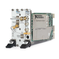
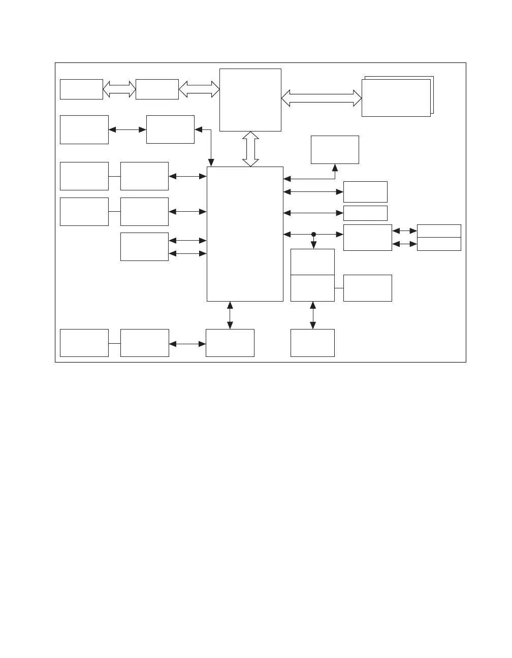
Figure 1-1. NI PXI-8109 Block Diagram
The NI PXI-8109 consists of the following logic blocks on the CPU
module and the I/O module. The CPU module has the following logic
blocks:
• FPGA 988A Socket is the socket definition for the Intel Core i7
processor.
• The SO-DIMM block consists of two 64-bit DDR3 SDRAM sockets
that can hold up to 4 GB each.
• The CPU connects to the DDR3 SDRAM, TI XIO2001 bridge, and
Intel 5 Series chipset.
• The SMB to PXI Trigger provides a routable connection of the PXI
triggers to/from the SMB on the front panel.
• The ATI Radeon E2400 Embedded GPU drives the graphics.
• The Watchdog Timer block consists of a watchdog timer that can reset
the controller or generate a trigger.
Intel
5 Series
Chipset
CPU
Intel Core
i7
SO-DIMM
DDR3 SDRAM
PC3 8500
DVI/VGA
Memory Bus Ch. A/B
Express
Card/34 Slot
x1 PCIE
USB
USB 2.0 x4
SATA
Hard Disk
FLASH
Watchdog
Trigger
SMB
Connector
Super I/O
LPT
COM1
x1
PXI
Triggers
GPIB
Controller
GPIB
Connector
USB 2.0 x4
Intel 82577
Gigabit
PHY
RJ45
Port 1
S ATA
x4 DMI
GPU ATI
Radeon
E2400
DVI-I
x4
PCIE
LPC
TI XIO2001
Bridge
PXI
Intel 82574
Gigabit
MAC/PHY
RJ45
Port 2
x1 PCIE
SPI
PCI
x1 PCIE
 Loading...