A-25
Appendices
NJ-series CPU Unit Hardware User’s Manual (W500)
A-2 Specifications of Basic I/O Units
A
A-2-2 Basic I/O Units
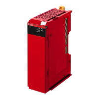
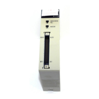
CJ1W-OD213 Transistor Output Unit (16 Points)
* Terminal numbers A0 to A8 and B0 to B8 are used in the external connection and terminal-device variable diagrams. They
are not printed on the Units.
Name 16-point Transistor Output Unit with Terminal Block (Sinking Outputs)
Model CJ1W-OD213
Rated Voltage 24 VDC
Operating Load Voltage Range 20.4 to 26.4 VDC
Maximum Load Current 0.5 A/point, 5.0 A/Unit
Maximum Inrush Current 4.0 A/point, 10 ms max.
Leakage Current 0.1 mA max.
Residual Voltage 1.5 V max.
ON Response Time 15 s max.
OFF Response Time 80 s max.
Insulation Resistance 20 M between the external terminals and the GR terminal (100 VDC)
Dielectric Strength
1,000 VAC between the external terminals and the GR terminal for 1 minute at a leakage current of
10 mA max.
Number of Circuits 16 (16 points/common, 1 circuit)
Internal Current Consumption 5 VDC 150 mA max.
Fuse None
External Power Supply 20.4 to 26.4 VDC, 55 mA min.
Weight 110 g max.
Circuit Configuration
External connection and terminal-
device variable diagram
• When wiring, pay careful attention to the polarity of the external power supply. The load may oper-
ate incorrectly if the polarity is reversed.
Output indicator
Internal circuits
to
Signal
name
Jxx_Ch1_Out00
+V
Jxx_Ch1_Out15
COM
24 VDC
Signal
name
Signal
name
Connec-
tor pin
*
B1
B2
B3
B4
B5
B6
B7
B8
A1
A2
A3
A4
A5
A6
A7
A8
B0
A0
L
L
L
L
L
L
L
L
L
L
L
L
L
L
L
L
Jxx_Ch1_Out01
Jxx_Ch1_Out03
Jxx_Ch1_Out05
Jxx_Ch1_Out07
Jxx_Ch1_Out09
Jxx_Ch1_Out11
Jxx_Ch1_Out13
Jxx_Ch1_Out15
Jxx_Ch1_Out00
Jxx_Ch1_Out02
Jxx_Ch1_Out04
Jxx_Ch1_Out06
Jxx_Ch1_Out08
Jxx_Ch1_Out10
Jxx_Ch1_Out12
Jxx_Ch1_Out14
COM
+V
 Loading...