96
Wiring Section 3-3
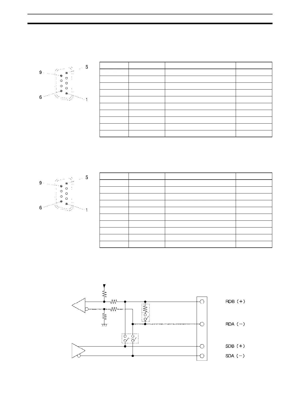
3-3-4 Connector Pin Layout
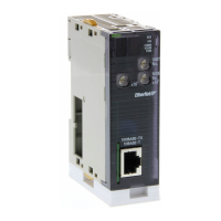
RS-232C Ports This layout applies to the following ports: ports 1 and 2 of the CS1W-SCB21-
V1/SCU21-V1, ports 1 and 2 of the CJ1W-SCU21-V1, port 1 of the CS1W-
SCB41-V1, and port 2 of the CJ1W-SCU41-V1.
Refer to 2-1 Component Names and Functions for signal precautions.
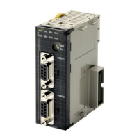
RS-422A/485 Ports This layout applies to the following ports: port 2 of the CS1W-SCB41-V1,
ports 1 and 2 of the CS1W-SCU31-V1, ports 1 and 2 of the CJ1W-SCU31-V1,
and port 1 of the CJ1W-SCU41-V1.
Note When the 2-wire connections are used, use either pins 1 and 2, or pins 6 and
8.
Refer to 2-1 Component Names and Functions for signal precautions.
The internal circuits are shown in the following diagram.
Pin Abbreviation Signal name I/O
1 FG Shield ---
2 SD Send data Output
3 RD Receive data Input
4 RTS (RS) Request to send Output
5 CTS (CS) Clear to send Input
6 5V Power supply ---
7 DSR (DR) Data set ready Input
8 DTR (ER) Data terminal ready Output
9 SG Signal ground ---
Hood FG Shield ---
Pin Abbreviation Signal name I/O
1 SDA Send data - Output
2 SDB Send data + Output
3 NC Unused ---
4 NC Unused ---
5 NC Unused ---
6 RDA Receive data - Input
7 NC Unused ---
8 RDB Receive data + Input
9 NC Unused ---
Hood FG Shield ---
Receiver
Driver
Pin 1
Pin 2
Pin 6
Pin 8
Terminating resistance: 220 Ω ∗
Terminating resistance switch
2-wire or 4-wire switch
Port 2
∗ When connecting to a MODBUS device, turn OFF the terminating resistance switch and
connect terminating resistance according to the specifications of the external device.
51 KΩ
4.7 KΩ
4.7 KΩ
51 KΩ
 Loading...