NB-IoT Module Series
BC95 Hardware Design
BC95_Hardware_Design Confidential / Released 32 / 51
BC95 provides an RF antenna pad for antenna connection. There is one grounding pad on both sides of
the antenna pad in order to give a better grounding. Besides, a π-type match circuit is suggested to be
used to adjust the RF performance, and place the π-type matching components as close to the antenna
as possible.
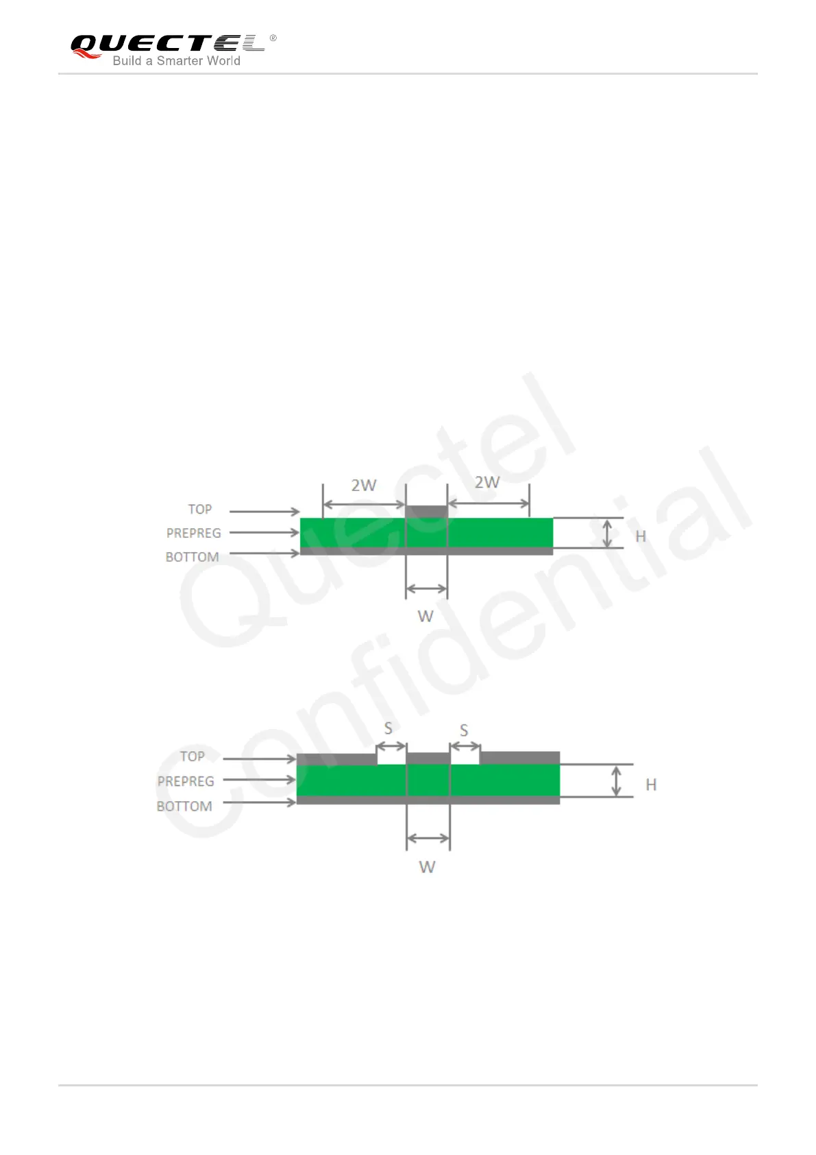
4.2. Reference Design of RF Layout
For user’s PCB, the characteristic impedance of all RF traces should be controlled as 50 ohm. The
impedance of the RF traces is usually determined by the trace width (W), the materials’ dielectric constant,
the distance between signal layer and reference ground (H), and the clearance between RF trace and
ground (S). Microstrip line or coplanar waveguide line is typically used in RF layout for characteristic
impedance control. The following are reference designs of microstrip line or coplanar waveguide line with
different PCB structures.
Figure 17: Microstrip Line Design on a 2-layer PCB
Figure 18: Coplanar Waveguide Line Design on a 2-layer PCB
 Loading...