EasyManuals Logo
Home>Quectel>Control Unit>BG96

Quectel BG96 User Manual

Quectel BG96
80 pages
To Next Page IconTo Next Page
To Previous Page IconTo Previous Page
Page #15 background imageLoading...
Page #15 background image
LPWA Module Series
BG96 Hardware Design
BG96_Hardware_Design 14 / 79
3.
2)
Within extended temperature range, the module remains the ability to establish and maintain a
voice, SMS, data transmission, emergency call, etc. There is no unrecoverable malfunction. There
are also no effects on radio spectrum and no harm to radio network. Only one or more parameters like
P
out
might reduce in their value and exceed the specified tolerances. When the temperature returns to
the normal operating temperature levels, the module will meet 3GPP specifications again.
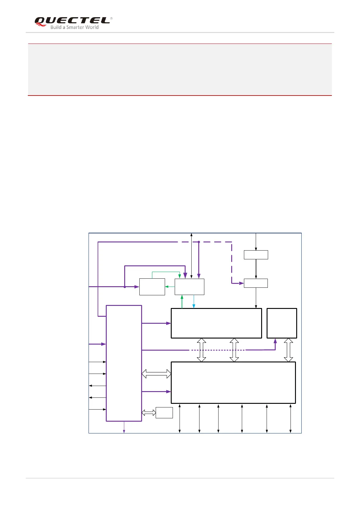
2.3. Functional Diagram
The following figure shows a block diagram of BG96 and illustrates the major functional parts.
Power management
Baseband
DDR+NAND flash
Radio frequency
Peripheral interfaces
Baseband
PMIC
Transceiver
NAND
DDR2
SDRAM
PA
(2G+ASM)
SAW
ANT_MAIN
ANT_GNSS
VBAT_BB
VBAT_RF
PWRKEY
VDD_EXT
USB
(U)SIM PCM
I2C
RESET_N
19.2M
XO
STATUS
GPIOs
Control
IQ Control
LNA
Tx
Rx
GNSS
UARTs
NETLIGHT
PA
(4G)
ADCs
Figure 1: Functional Diagram

Table of Contents

Other manuals for Quectel BG96

Questions and Answers:

Question and Answer IconNeed help?

Do you have a question about the Quectel BG96 and is the answer not in the manual?

Quectel BG96 Specifications

General IconGeneral
BrandQuectel
ModelBG96
CategoryControl Unit
LanguageEnglish

Related product manuals