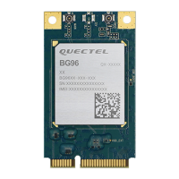
LPWA Module Series
BG96 Hardware Design
BG96_Hardware_Design 62 / 79
1.
1)
“Typ.” value means the average current consumption value.
2.
2)
“Rock Bottom Sleep” means the operation is performed with AT+CFUN=0 and AT+QSLCK=1 (DTR
pin at high level).
3.
3)
Sleep state with UART connected and USB disconnected. The module can enter sleep mode
through executing AT+QSCLK=1 command via UART interface and then controlling the module’s
DTR pin. For details, please refer to Chapter 3.4.4.
4. LTE-FDD B25 is supported on BG96 of R1.2 hardware version.
Table 35: GNSS Current Consumption
6.5. RF Output Power
The following table shows the RF output power of BG96 module.
Table 36: BG96 RF Output Power
Cold Start @Passive Antenna
Lost State @Passive Antenna
Open Sky @Passive Antenna
LTE-FDD B1/B2/B3/B4/B5/B8/B12/B13/B18/B19/B20/B25/
B26/B28

 Loading...