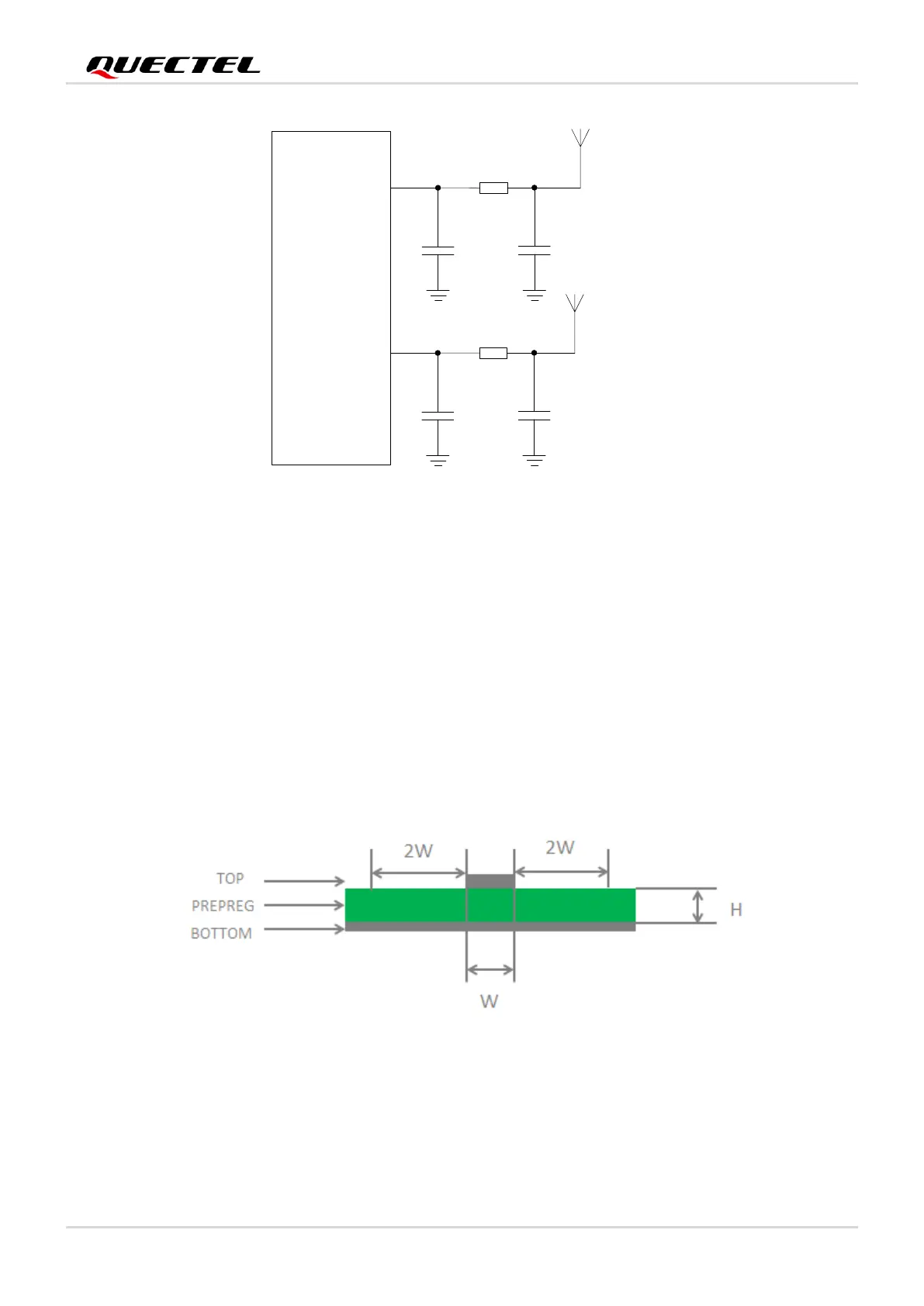
Figure 28: Reference Circuit of RF Antenna
5.1.4. Operating Frequency
For user’s PCB, the characteristic impedance of all RF traces should be controlled as 50 Ω. The
impedance of the RF traces is usually determined by the trace width (W), the materials’ dielectric constant,
the height from the reference ground to the signal layer (H), and the spacing between the RF traces and
the ground (S). Microstrip or coplanar waveguide is typically used in RF layout to control characteristic
impedance. The following are reference designs of microstrip or coplanar waveguide with different PCB
structures.
.
Figure 29: Microstrip Design on a 2-layer PCB

 Loading...