EasyManuals Logo
Home>Quectel>GSM/GPRS Modules>LPWA Series

Quectel LPWA Series Hardware Design

Quectel LPWA Series
90 pages
To Next Page IconTo Next Page
To Previous Page IconTo Previous Page
Page #44 background imageLoading...
Page #44 background image
LPWA Module Series
BG950A-GL&BG951A-GL_Hardware_Design
43
/89
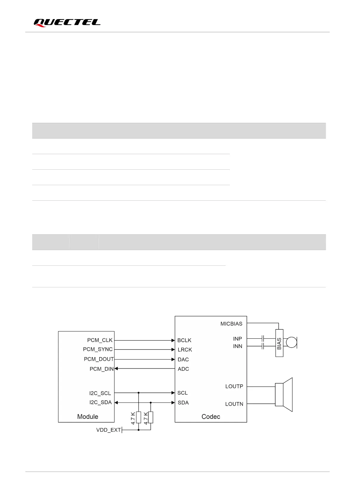
4.3. PCM and I2C Interfaces*
The module provides one Pulse Code Modulation (PCM) digital interface and one I2C interface for
VoLTE* only. The PCM interface supports the following modes:
Table 14: Pin Definition of PCM Interface
Table 15: Pin Definition of I2C Interface
The reference design is illustrated as follows:
Figure 17: Reference Circuit of PCM Interface
Pin Name
Pin No.
I/O
Description
Comment
PCM_CLK
4
DO
PCM clock
1.8 V power domain.
If unused, keep this pin open.
PCM_SYNC
5
DO
PCM data frame sync
PCM_DIN
6
DI
PCM data input
PCM_DOUT
7
DO
PCM data output
Pin Name
Pin No.
I/O
Description
Comment
I2C_SCL
40
OD
I2C serial clock (for external codec)
External pull-up resistor is
required.
1.8 V only.
If unused, keep this pin open.
I2C_SDA
41
OD
I2C serial data (for external codec)

Table of Contents

Other manuals for Quectel LPWA Series

Questions and Answers:

Question and Answer IconNeed help?

Do you have a question about the Quectel LPWA Series and is the answer not in the manual?

Quectel LPWA Series Specifications

General IconGeneral
BrandQuectel
ModelLPWA Series
CategoryGSM/GPRS Modules
LanguageEnglish

Related product manuals