LPWA Module Series
BG950A-GL&BG951A-GL_Hardware_Design
46
/89
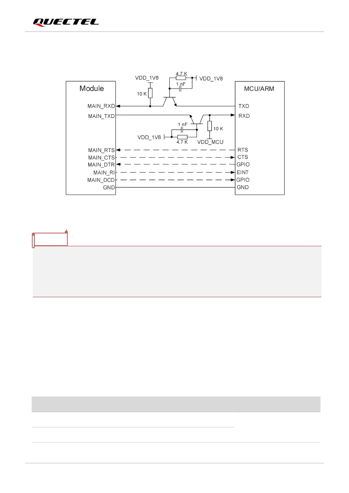
Another example with transistor circuit is shown as below. For the design of circuits shown in dotted
lines, refer to that shown in solid lines, but pay attention to the direction of connection.
Figure 19: Reference Circuit with Transistor Circuit
4.5. ADC Interface
The module provides two Analog-to-Digital Converter (ADC) interfaces. To improve the accuracy of ADC,
the trace of ADC interfaces should be surrounded by ground.
Table 20: Pin Definition of ADC Interface
1. Transistor circuit solution is not suitable for applications with high baud rates exceeding 460 kbps.
2. The main UART of the module shouldn’t be asserted high during BG950A-GL & BG951A-GL enter
PSM.
3. Please note that the module CTS is connected to the host CTS, and the module RTS is connected
to the host RTS.
General-purpose ADC interface
General-purpose ADC interface

 Loading...