Renesas RA Family EK-RA6M5 v1 – User's Manual
R20UT4829EG0100 Rev. 1.00 Page 12 of 34
Mar.15.21
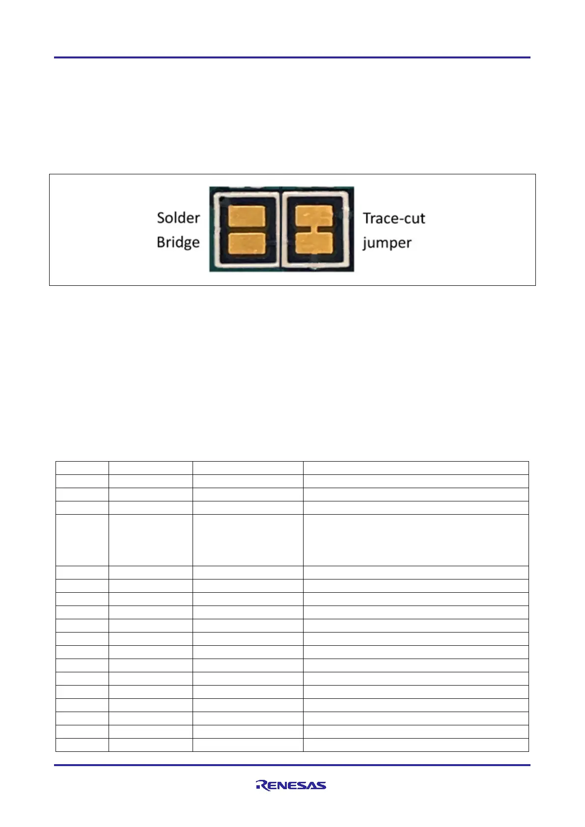
• Solder may be applied to both pads to develop a bulge on each and the bulges joined by touching a
soldering iron across the two pads.
• A small wire may be placed across the two pads and soldered in place.
• A SMT resistor, size 0805, 0603, or 0402, may be placed across the two pads and soldered in place. A
zero-ohm resistor shorts the pads together.
For any copper jumper, the connection is considered closed if there is an electrical connection between the
pads (default for trace-cut jumpers.) The connection is considered open if there is no electrical connection
between the pads (default for the solder-bridge jumpers.)
Figure 6. Copper Jumpers
4.3.2 Traditional Pin Header Jumpers
These jumpers are traditional small pitch jumpers that require an external shunt to open/close them. The
traditional pin jumpers on the EK-RA6M5 board are 2 mm pitch headers and require compatible 2 mm shunt
jumpers.
4.3.3 Default Jumper Configuration
The following table describes the default settings for each jumper on the EK-RA6M5 board. This includes
copper jumpers (Ex designation) and traditional pin jumpers (Jx designation.)
The Circuit Group for each jumper is the designation found in the board schematic (available in the Design
Package). Functional details for many of the listed jumpers may be found in sections associated with each
functional area of the kits.
Table 1. Default Jumper Settings
Configures J-Link OB connection to MCU mode
Configures the MCU for normal operation
Configures Reset# for on-board debugger mode
Jumper on pins 3-4
Jumper on pins 5-6
Connects the J-Link OB debugger to the RA
MCU
Configures the MCU for normal boot mode
Sets USB FS power to device mode
Connects micro-USB power to system power
Sets USB HS power to device mode
Connects micro-USB power to system power
Connects VREFH0 to +3.3 V
Connects P212/EXTAL to 24 MHz crystal
Connects P213/XTAL to 24 MHz crystal
Connects P213/XTAL pin to pin headers

 Loading...


